
To meet the growing demands of next-generation mobile devices—featuring more functions, multiple communication modes, and a wide range of operating frequencies—engineers are increasingly focused on enhancing RF front-end integration. By leveraging advanced integration techniques within CMOS processes, they have found effective solutions to this complex challenge.
As consumer expectations continue to rise, there is a strong push for smaller, more affordable handsets and portable devices that support high-speed wireless data services and multi-mode capabilities. The evolution of 2.5G (GPRS, CDMA 1xRTT) and 3G (UMTS/W-CDMA, cdma2000) networks has enabled faster data transmission, while the use of optimized silicon processes and key components like integrated RF transceivers helps reduce both size and cost in mobile devices.
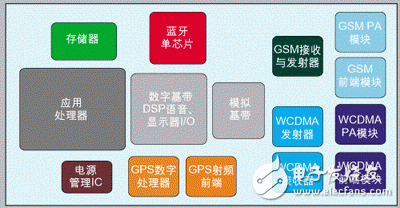
*Figure 1: Common wireless subsystems found in multimodal platforms.*
Mobile phone manufacturers often combine various technologies to create competitive products tailored for specific markets. For instance, devices supporting GSM, GPRS, EDGE, and W-CDMA allow users to access multiple high-speed networks through a single device, showcasing the core concept of multi-mode technology. Additional features such as GPS, Bluetooth, and even WLAN are also commonly integrated into modern smartphones.
Most multi-mode platforms today consist of several independent wireless subsystems built on a shared platform, as illustrated in Figure 1. A typical example includes handsets that support GSM, W-CDMA, Bluetooth, and GPS. These systems may include separate baseband chips, application processors, power management ICs, memory ICs, RF transceivers, and discrete components for each wireless function.
In such designs, single-chip Bluetooth and dual-chip GPS modules are typically connected to the application processor, with their drivers embedded in the operating system. Because these subsystems operate independently, they can run in parallel during network calls or other tasks.
While system-level integration offers benefits for some applications, it may not always be the most cost-effective or space-efficient approach. The final stage of integration usually occurs at the component level, including the RF front-end, baseband, and transceiver.
**Integrated RF Front-End System**
GSM-based phones using time-division duplexing typically require only switches in their RF front-end. A basic single-band GSM phone needs a single-pole double-throw switch, a receiver filter, and matching network along with a power amplifier. However, the demand for more feature-rich phones has pushed GSM support to cover up to four frequency bands. This means a quad-band GSM handset may have four transmit channels and four receive channels, significantly increasing complexity.
Each transmit channel requires at least two amplifiers—one for GSM850/GSM900 and another for DCS-1800/PCS-1900. Adding filters and passive components for the receive channels brings the total to six, making the design more complex and increasing the number of components.
When adding a second wireless system, such as 802.11b WLAN, to the same platform, the challenge of adding functionality without increasing design complexity or cost becomes more significant. Since GSM and 802.11b operate on different frequency bands, their front-end components cannot be shared. Therefore, both systems need their own power amplifiers, switch networks, receiver matching circuits, and filters.
The best way to manage this is by using pre-integrated modules and packages. Multi-chip power amplifier modules with built-in power control logic are already used in multi-band handsets and multi-mode WLAN applications. Similarly, RF front-end modules containing switch networks and receive filters are also available. In the future, we may see fully integrated RF front-end subsystems that combine cellular and WLAN functionalities.
**Baseband Split**
Many current baseband chips are highly integrated CMOS system-on-chips (SoCs), which either combine digital and analog functions or split them into separate chips. The choice between these approaches depends on factors like future integration possibilities.
The two-chip solution is particularly advantageous because it isolates analog baseband functions from the "pure" digital circuits of the digital baseband. This allows digital basebands to benefit from smaller CMOS geometries as per Moore’s Law, which is challenging for analog circuits.
Another benefit of this split is the ability to integrate other digital CMOS components, such as application processors, image processors, and memories, into one SoC. With the development of digital RF interfaces, such as those defined by DigRF standards, analog circuits may eventually disappear from the baseband entirely.
This approach promotes a standardized high-speed digital serial interface between the radio and the baseband. Similar efforts are underway among WLAN vendors, with JEDEC 61 defining standard serial interfaces. Once these interfaces are standardized, integrating cellular baseband functions with complementary digital features or other wireless baseband circuits will become more efficient and cost-effective.
**RF Transceiver Integration in CMOS**
The integration of RF transceivers in CMOS technology continues to evolve, offering new opportunities for miniaturization and performance improvements. As the industry moves toward more advanced nodes, the ability to implement complex RF functions on a single chip becomes increasingly feasible. This trend is expected to drive further innovation in multi-mode and multi-band mobile devices.
Energy 5000 Puffs,Rechargeable Vape 5000 Puffs,Energy Drink Disposable Vape,Energy 5000Puffs Disposable Vape
YIWU JUHE TRADING COMPANY , https://www.nx-vapes.com