
As the demand for more advanced features, multiple communication modes, and broader frequency support in next-generation mobile devices continues to rise, engineers are increasingly focused on enhancing RF front-end integration. Leveraging cutting-edge CMOS-based integration solutions has become a key strategy in addressing these challenges effectively.
Consumer expectations for compact, affordable handsets with high-speed wireless data capabilities and multi-mode support are driving significant growth in the mobile phone market. The evolution of 2.5G (GPRS, CDMA 1xRTT) and 3G (UMTS/W-CDMA, cdma2000) networks has enabled faster data transmission, while the use of advanced silicon processes and integrated RF transceivers helps reduce both the size and cost of mobile devices.
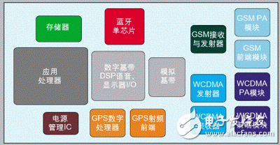
Figure 1: Common wireless subsystems found in multi-mode platforms.
Mobile phone manufacturers integrate various technologies to offer competitive solutions tailored for specific markets. For instance, devices supporting GSM, GPRS, EDGE, and W-CDMA allow users to access multiple high-speed networks through a single device, which is a fundamental application of multi-mode technology. Additional features like GPS, Bluetooth, and Wi-Fi are also commonly integrated into modern handsets.
Most multi-mode platforms today consist of multiple independent wireless subsystems built on a shared platform, as illustrated in Figure 1. For example, a multi-mode handset supporting GSM, W-CDMA, Bluetooth, and GPS may include a GSM/W-CDMA baseband, an application processor, power management IC, memory IC, separate RF transceivers, a single-chip Bluetooth system, a dual-chip GPS module, and a multi-mode RF front-end with passive components.
In such a setup, the Bluetooth and GPS chipsets are connected to the application processor, with their drivers embedded in the operating system that manages the entire platform. These standalone systems can operate in parallel during network calls, offering seamless performance.
While integrating multiple wireless functions at the system level makes sense for certain applications, it doesn't always provide the most cost-effective or space-efficient solution. The ultimate goal is to achieve full integration at the component level, including the RF front end, baseband, and transceiver.
Integrated RF Front-End System
GSM-based phones using time-division duplexing typically require only switches in their RF front-end systems. A basic single-band GSM phone needs just a single-pole double-throw switch, a receiver filter, and matching network, along with a power amplifier. However, with the growing demand for feature-rich devices, modern GSM phones must now support up to four frequency bands, increasing complexity significantly.
A quad-band GSM handset may have up to four transmit and receive channels, requiring at least two power amplifiers—one for the lower bands (GSM850/GSM900) and another for the higher bands (DCS-1800/PCS-1900). Adding filters and passive components for the receive channel results in a total of six channels, complicating the design and increasing the number of components used.
When adding a second wireless system, such as 802.11b WLAN, to the same platform, the challenge becomes even greater. Since GSM and WLAN operate on different frequency bands, they cannot share front-end components. This means each mode requires its own set of power amplifiers, switches, receiver matching circuits, and filters. To manage this complexity, pre-integrated modules and packages are often used.
Multi-chip power amplifier modules with built-in power control logic are already being used in multi-band handsets and multi-mode WLAN applications. Similarly, RF front-end modules containing switch networks and receive filters are also available. In the future, we may see fully integrated RF front-end subsystems that combine cellular and WLAN functionalities.
Baseband Splitting
Many current cellular baseband chips are highly integrated CMOS SoCs, either combining digital and analog functions on a single chip or separating them into two distinct chips. The choice between these options depends on factors such as future integration potential.
The two-chip approach is often preferred because it isolates analog baseband functions from the digital circuits, allowing the digital baseband to benefit from smaller CMOS geometries as per Moore’s Law. This separation also enables the integration of other digital CMOS components, such as application processors and memories, into one of the SoCs.
With the emergence of digital RF interfaces—such as those defined by the DigRF standards organization—analogue circuits in the baseband could eventually be eliminated. This approach promotes a standardized high-speed digital serial interface between the radio and the baseband, making integration more efficient.
Similar standardization efforts are underway in the WLAN industry, with organizations like JEDEC working on defining standard serial interfaces. Once these interfaces are established, cellular baseband functionality can be more easily combined with other digital functions or wireless modes, reducing costs and improving performance.
RF Transceiver Integration in CMOS
YIWU JUHE TRADING COMPANY , https://www.nx-vapes.com