
Li Qiaoyang, China Institute of Aeronautical Computing Technology
[Keywords] "three" module; PowerPC8270; PMC
1 Introduction
With the rapid development of the aviation field, the development of airborne computers continues to evolve, resulting in a generalized, serialized and modular (modular) product standard system, namely, a "three-in-one" product system. Generalization refers to the adoption of open architecture and general-purpose and mature industrial technologies, including general industrial standards and specifications, as well as industrial-grade components and the like, to shorten the procurement cycle of avionics systems, reduce research and development costs, and effectively solve the problem of the suspension of production of military devices. The smooth insertion problem guarantees the system's ability to upgrade and expand; serialization refers to the realization that products with different performance levels are allowed through an open architecture, to achieve continuous development and continuous upgrade of avionics and achieve product serialization; Reasonable combination of modules and functions to achieve the optimal combination, including the gradual approach to the industrialization of the standard system in terms of size, functional penetration into smaller functional circuit blocks, to achieve the optimal combination of modules and functional circuits.
The standard PMC module (PC8270) based on PowerPC8270 processor is a high-performance, highly reliable, low-power airborne embedded processing module. The PMC standard architecture design, in line with the generalization, serialization, combination of "three" design requirements, is a high-performance COTS (commercial shelf product) module.
2. Overview
The PowerPC8270 processor is a high-performance 32-bit RISC processor from the Freescale PowerUICC II family based on the PowerPC 603e core. This series of chips supports a wide range of protocols and interfaces, including 3 Fast Ethernet, ATM, HCLC, and 4 SCCs. Interfaces, 2 SMC interfaces, a 32-bit 33/66 MHz PCI bus interface, and a USB host/device interface. The processor is a dual processor core, an embedded PowerPC 603e core and a communications processing module (CPM), dual address bus, 32-bit local bus and 64-bit 60x bus (64-bit data bus, 32 address lines), bus clock Maximum support 100MHz. Low power consumption, typical power consumption at 400M/300M/100M frequency is 1.5W, maximum power consumption is 1.65W.
The PowerPC 8270 series integrates two processing units: an embedded PowerPC 603e core and a reduced instruction set (RISC) communication processing module (CPM). This dual-core design can reduce power consumption and provide more balanced processing power than traditional designs. The CPM is responsible for the underlying peripheral communications tasks, while the 603e core is focused on managing internal processing tasks. Its extensive protocol stack support capability is the biggest highlight of the series.
3. System Structure
PC8270 high-performance processing module uses a PowerPC 8270 as the main processor, processing core frequency 450M/300M/100MHz. The processor has independent storage resources: SDRAM, FLASH, NVSRAM. On the module, the control logic of the local bus of the processor is realized by the programmable control logic device. At the same time, 12 PortC interfaces are realized through the FPGA, and the interruption control of the module is realized. The processor outputs two 10M/100M Ethernet interfaces to the PMC socket for commissioning and maintenance of the module. The PCI interface of the processor is connected to the PMC socket to communicate with other modules on the PCI bus. The module outputs 2 RS232 interfaces and 2 RS422 interfaces externally, all connected to the PMC socket. Among them, 2 RS232 interfaces are used for debugging and maintenance, and 2 RS422 interfaces are used as low-speed communication buses. The block diagram of the PC8270 module is shown in Figure 1.

Figure 1 PC8270 module structure
4. Hardware circuit design
4.1 Power Conversion Circuit
The module uses an external +5V power supply. The processor PowerPC8270 core voltage is 1.5V, the interface voltage is 3.3V, the core voltage of the FPGA is 1.2V, the interface voltage is 3.3V, other chips are 5V or 3.3V voltage input. The interface voltage of 3.3V is provided by the switching power supply LTM4600 and the maximum current is 10.0A. The 1.2V power supply for the FPGA core and 1.5V for the CPU core supply are small and are provided using the TPS74401, as shown in Figure 2.
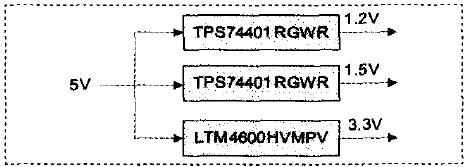
Figure 2 power conversion circuit
4.2 Processor circuit
In this design, the processor model uses MPC8270C ZUUPEA (-40°C to +105°C) and the package is 48O1BGA. The CPU and SDRAM speeds are respectively 400MHz and 66MHz. The PCI configuration of the processor is PCI host and the bus frequency is 66MHz. The operating frequency of the processor can be configured through the FPGA.
The PowerPC8270 power-on reset signal is provided by Maxim's MAX706. An external reset signal is introduced from the PMC socket, as shown in Figure 3. After power-up, the FPGA is loaded with logic, the DONE signal is low, the MAX706 resets the output pin to a low level, and the entire module is in a reset state; after the logic load ends, the DONE signal goes high and the MAX706 resets the output pin. After a delay of 200ms, it goes high and the entire module is in normal operation. In addition, the system provides a soft reset function to reset the PC8270 through software write registers. The PCI reset signal is issued by the CPU and resets other PCI devices.

Figure 3 reset circuit
4.3 Memory Circuit
The module configures memory cells with an integrated 60x bus controller.
4.3.1 Boot FLASH Memory
The module provides 16-bit wide 32Mbytes of Boot FLASH memory for storing the PC8270 module power-on boot program, module power-on self-test (PUBIT) program, Vxworks operating system core code image. The Boot FLASH memory is implemented with a SSPANGL S29GL256P10TFI010. The operating voltage is 3.3V. The package is a 56-pin TSOP with a capacity of 32 Mbytes. It supports whole erase and write and sector write protection.
4.3.2 User FLAsH Memory
The CPU module provides 16-bit wide 32Mbytes of USER FLASH memory for storing applications. The USER FLASH memory is implemented using a Spanview S29GL256P10TFI010. The operating voltage is 3.3V. The package is a 56-pin TSOP with a capacity of 32Mbytes. It supports whole erase and write and sector write protection.
4.3.3 SDRAM memory
The CPU module provides a 72-bit data width (of which 8 bits are ECC check bits) 128 Mbyte of SDRAM operating at 66 MHz. SDRAM is implemented using five TWSD1616 (4M*16*4) domestic 871 factories, one of which implements 8-bit ECC check, operates at 3.3V and is packaged as 64-pin CLCC.
4.3.4 NVSRAM memory
The CPU module provides 128Kbytes of NVSRAM. The device uses a STK company’s STK14CA8-NF45I, 8-bit data width, and an operating voltage of 3.3V. NVSRAM is used for power-down data protection. There are 128KB of SRAM and 128KB of EEPROM in each chip. When the power is turned off, the data in SRAM is written into EEPROM by using the power of large-capacity tantalum capacitor. When power is turned on, SRAM is automatically written from EEPROM. In the recovery of power-down data.
4.4 PCI bus interface
The PCI total interface is implemented using the PCI interface provided by the MPC8270 chip. The operating level is 3.3V, the transmission clock is 66MHz, and the host mode supports single-byte operation and Burst operation. The processor communicates with other devices on the PCI bus through the PMC socket.
4.5 FPGA circuit
One FPGA chip is used to implement the interface logic control function on the module. The chip selects XA Spartan3A series chip XC3S2OOAN-4FTG256I from Xilinx Company to implement the module's reset control, interrupt management, processor local bus access control, watchdog timer, and discrete control. And module control status register to achieve other functions.
4.6 Watchdog Timer
The watchdog circuit is implemented using FPGA. When the watchdog feeds the dog, the watchdog interrupt occurs. When the watchdog circuit generates three consecutive watchdog interrupts and none of them are processed, the watchdog circuit issues a watchdog reset. The system is in the air state. The watchdog circuit is automatically enabled after being powered on and cannot be disabled. When GSE* is low, the system is in the ground debug and maintenance state. The watchdog circuit is controlled by the software enable bit WDOEN. WDOEN is When '0' is enabled, the watchdog is enabled. When WDOEN is '1', the watchdog is disabled. After the watchdog circuit generates an interrupt, it is sent to the interrupt circuit and also to the channel fault logic circuit. In normal use, the user is required to generate the watchdog timer clear signal within the watchdog timer period and clear the watchdog timer. The watchdog timing period can be set by software.
4.7 Other circuits
The integrated debugging interface is realized by using a 25-core J63A-2F2-025-431-TH curved plug board socket of a domestic 3419 factory. The integrated debug interface integrates the FPGA JTAG interface and processor. The JTAG interface is used to debug the hardware of the module. The position of the interface is placed on the top of the module to facilitate debugging of the module in the system.
The RTC is implemented by a DS1374C chip from Dallas. It is connected to the peripheral bus of the main processing node to provide date and time information for the system.
5. Structural design
The physical composition and external dimensions of the module meet the requirements of the PMC standard daughter card specification. Its physical properties are as follows: Printed circuit board dimensions: length × width × thickness = (143.75mm ± 0.20mm) × (74.00mm ± 0.20mm) × (2.0 Mm ± 0.2mm).
6. Software design
The configuration software for the PC8270 module includes boot boot programs, operating systems, driver packages, and FLASH programming tools.
6.1 Boot Boot Program
The boot program is the program module that is executed first after the system is powered on. It is responsible for the system control from system power on to the system entering a certain working state. The functional modules of the CPU module boot program include: a system initialization module, a branch (working state) determination module, a system parameter configuration module, and a solidification support module.
6.2 Operating System
The module is equipped with PowerPC8270 processor for the United States Wind River's VxWorks5.5 embedded real-time operating system (RTOS), to meet the communication, military, aerospace and other real-time requirements of the embedded field applications.
6.3 Driver Package
Drivers running on the module include memory drivers, watchdog timer drivers, interrupt controllers, and PCI bus drivers.
6.4 FLASH programming tool
The FLASH programming tool provides online solidification of the software code to program the FLASH. The programming data can be loaded via Ethernet or serial port to facilitate the user to update the software code on the FLASH.
7. Conclusion
The rapid development of the aviation field puts forward higher requirements for embedded airborne computer technology, combined with generalization, serialization, and combination of "three" design requirements. This paper presents a design of a high performance and low power standard PMC processing module. Implement the plan. This module complies with the PMC standard, has high-performance data processing performance, rich communication interface support, lower power consumption, can meet the high-performance, multi-task, low-power processing requirements of the new generation of embedded electronic systems, and can be widely used Highly reliable airborne embedded field.
Spring Clamp Terminal Block,Spring Terminal Connector,Spring Loaded Terminal Blocks,Spring Cage Terminal Block
Cixi Xinke Electronic Technology Co., Ltd. , https://www.cxxinke.com