
The ADC16V130 from NS is a high-performance 16-bit analog-to-digital converter (ADC) capable of sampling at up to 130 million samples per second (MSPS), featuring LVDS output. It operates on dual power supplies, +1.8V and +3.0V, offering excellent dynamic performance with a full-power bandwidth of 1.4 GHz, a signal-to-noise ratio (SNR) of up to 76.7 dBFS, and a spurious-free dynamic range (SFDR) of 90.6 dBFS. The ADC16V130 is widely used in high intermediate frequency (IF) sampling receivers, multi-carrier base station receivers, test and measurement equipment, communication infrastructure, data acquisition systems, and portable instrumentation.
This paper provides an overview of the key features of the ADC16V130, including its block diagram, low-frequency and high-frequency transformer drive circuits, and the SP16130CH4RB low IF receiver reference design. It also includes detailed circuit diagrams and a complete bill of materials (BOM) for practical implementation.
The ADC16V130 is a monolithic CMOS ADC that converts analog input signals into 16-bit digital words at rates up to 130 MSPS. It uses a differential, pipelined architecture with built-in digital error correction and an on-chip sample-and-hold circuit, which helps reduce power consumption and external component count while maintaining superior dynamic performance. The device includes automatic power-up calibration to ensure consistent performance across different units, and it can be recalibrated at any time by asserting and then de-asserting the power-down pin.
An integrated low-noise voltage reference and differential reference buffer simplify board-level design, while an on-chip duty cycle stabilizer ensures minimal jitter and allows for a wide input clock duty cycle without affecting performance. The unique sample-and-hold stage provides a full-power bandwidth of 1.4 GHz, and the digital output is delivered via full-rate LVDS ports, making it suitable for the compact 64-pin LLP package (9mm x 9mm).
The ADC16V130 offers several key features such as dual supply operation (1.8V and 3.0V), on-chip automatic calibration, low power consumption, multi-function pins for CLK/DF and PD, power-down and sleep modes, on-chip precision reference and sample-and-hold circuit, low-jitter duty-cycle stabilizer, full data rate LVDS output, and a small 64-pin LLP package. Its main specifications include a resolution of 16 bits, a conversion rate of 130 MSPS, SNR values of 78.5 dBFS (at 10 MHz), 77.8 dBFS (at 70 MHz), and 76.7 dBFS (at 160 MHz), SFDR of 95.5 dBFS (at 10 MHz), 92.0 dBFS (at 70 MHz), and 90.6 dBFS (at 160 MHz), and total power consumption of 755 mW (typical). It operates over a temperature range of -40°C to +85°C.
The ADC16V130 finds application in high IF sampling receivers, multi-carrier base station receivers supporting GSM/EDGE, CDMA2000, UMTS, LTE, and WiMax, test and measurement equipment, communications instrumentation, data acquisition systems, and portable instruments.
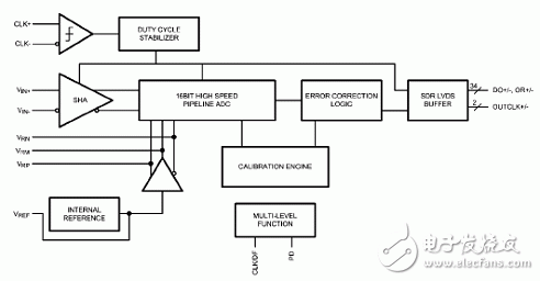
Figure 1. Block diagram of ADC16V130
Figure 2. ADC16V130 low frequency input transformer drive circuit
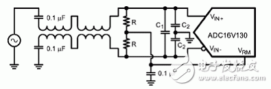
Figure 3. ADC16V130 high frequency input transformer drive circuit
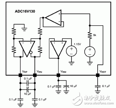
Figure 4. ADC16V130 internal reference and decoupling circuit
Aquarium Heaters,Aquarium Glass Heater,Glass Heaters For Aquarium,Aquarium Heaters Series
Sensen Group Co., Ltd.  , https://www.sunsunglobal.com