
I. Introduction
Integrated circuits (ICs) operating under harsh conditions continue to incorporate more and more functions, which requires improved device and circuit design strategies to increase robustness and minimize IC area. Due to stricter design, packaging and cost constraints, the protection architecture for applications such as FlexRay [1], local interconnect networks and control area network transceivers [2] is also being redesigned to reduce the number of additional protection components. To the lowest, while providing the required robustness. These robustness requirements include strict adherence to powered electrostatic discharge (ESD) and electromagnetic interference immunity requirements. To achieve a better transceiver architecture, it is best to choose a bidirectional blocking voltage clamp device that is compact and has high current handling capability. This is a challenge in advanced high pressure technology below 0.18 μm. In addition, these voltage-clamped devices must have a latch-up voltage slightly above ±45 V and a variable on-state hold voltage typically within ±(25–40) V.
The importance of protection devices for high-voltage bidirectional operation in the development of precision communication infrastructure interfaces is becoming increasingly apparent. Specifically, the single-chip two-dimensional control clamp device has a low hold voltage and a high quality factor (FOM) ratio (FOM refers to a maximum 100 ns transmission line pulse (TLP) per unit area), and is also presented in the consumer application literature. Define two-way blocking conditions [3], [4]. Current bi-directional devices have limitations in that it is difficult to adjust the bidirectional on-state holding voltage under high stress conditions without significantly reducing the response time and the performance of the clamp device. Attempts have been made to adjust the on-state holding voltage by substantially increasing the device pin pitch (such as the pitch of the emitter and collector in an NPN transistor) to meet stringent power-up ESD/EMI requirements [5]. In theory, the step recovery hold voltage of a bipolar transistor increases as the current gain decreases. This design adjustment is typically used for protection devices fabricated using traditional smart power technology [6]. On the other hand, increasing the device pin pitch can have a negative impact on the clamping performance, causing the clamp to slow down, increase the area, and cause parasitic devices to accidentally break down the substrate. An improved method can be effectively used for system optimization of automotive IC systems. The focus of optimization is on two-dimensional computer-aided design analysis of clamped bipolar latching features [7]. A new three-dimensional conduction control technique is introduced here to further optimize the balanced load injection during the on-state response of the device, which is helpful in understanding this method.
This paper presents a new approach to achieve bidirectional latching clamps. The complementary "T" shape and island are determined by forming a highly doped active region of the two pins of the clamp device, and the electron drive or hole drive small load current gain during the high level injection regeneration feedback is optimized without Increasing the spacing between the two pins results in a compact bidirectional high voltage latching clamp that maintains voltages between ±25 and ±40 V while also providing high current handling.
Second, the protection of the clamp device definition
Figure 1 (a) and (b) show partial perspective views of two-way hole-enhanced conductivity (BHEC) and electron-enhanced conductivity (BEEC) clamp devices, respectively. Simplified schematics are also shown and labeled in both configurations. The second pin (not shown) of the clamp device is constructed by creating a symmetric image in the "y" forward direction at the floating n-type regional interface formed by the H-NW and L-NW. The highly doped n+ and p+ active regions have a "T" shaped three-dimensional perspective array that enables optimal current gain adjustment for hole-driven or electronically driven small-load regeneration feedback and high-conductivity modulation at device startup.
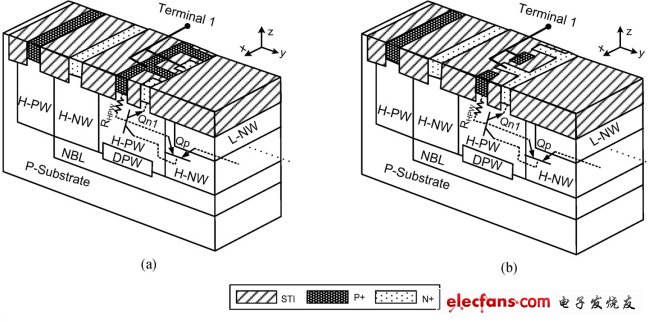
Figure 1, (a) Partial perspective and simplified schematic of a bidirectional clamp device with a hold voltage ≥ ± 40|V and (b) hold voltage ≥ ± 25|V.
Clamp devices appear as a simplified combination of standard implants, which are common in large bipolar CMOS–DMOS (BCD) advanced processes below 0.18 μm. In particular, the device can be optimized without additional process steps. The BHEC clamp device displays a set of isolated n+ effective area islands aligned with the "x" direction when viewed from above. The BHEC clamp device also includes a "T" shaped p+ implant and recombination active region, and an elongated portion extending in the "x" direction, and a set of projections extending from the "y" forward direction toward the central n-type region. The elongated portion is formed on the left side of the n+ effective region for enhancing hole injection and controlling in situ recombination. Each projection extends in the space between two corresponding n+ active area islands. The principle of the BEEC clamp device is the same, except that the "T" array and the island effective region definition are reversed to enhance the electron injection efficiency and increase the base resistance RHPW of the NPN transistor Qn1.
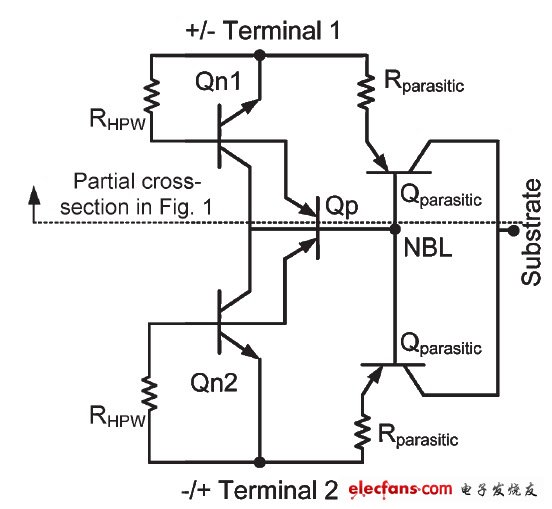
Figure 2, the equivalent schematic diagram of the bidirectional blocking voltage clamp device. The upper part of the dotted line is the equivalent schematic diagram of the partial view in Figure 1.
Figure 2 shows a detailed equivalent schematic of the structure of Figure 1. Note that the complementary "T" shape and island array used in the n+ and p+ active regions enhances the PNP action in Figure 1(a) and speeds up the response time of the NPN action in Figure 1(b). The relative change in bipolar action can be used to balance charge carrier injection and optimize bidirectional current-voltage (I–V) characteristics.
To elaborate on the structure of the schematic, at the first pin (Pin 1), the n+ and p+ active regions are in contact at the surface of the NPN bipolar Qn1 and correspond to the emitter and base regions. The p+ active region is also electrically connected to the p-type region formed by the H-PW and DPW regions. The DPW increases the doping concentration deep into the device, resulting in a breakdown voltage between the floating n-type region and the p-type region outside the surface. The p-type region determines the resistance RHPW and forms the emitter region of the PNP bipolar Qp.
Wall mount fiber termination boxes are designed for either pre-connectorized cables, field installation of connectors, or field splicing of pigtails. As usual it is also called Wall Mount Termination Box.Wall Mount Fiber Termination Box can distribute cables after installing splitters and draw out room fiber optic cables in direct or cross-connections.The Fiber Termination Box is suitable for fiber terminal point to complete connection, distribution and scheduling between perimeter fiber cables and terminal equipment.
Wall Mount Fiber Termination Box
Wall Mount Fiber Termination Box,Wall Mount Termination Box,Fiber Optic Box Wall,Variable Optical Attenuator
Foclink Co., Ltd , http://www.scfiberpigtail.com