
In a digital communication system, the transmitting end transmits each symbol in the digital pulse sequence one by one in a determined time sequence. At the receiving end, there must be an accurate sampling decision time to correctly determine the transmitted symbol. Therefore, the receiving end must provide a timing pulse sequence that determines the sampling decision timing. The repetition frequency of this timing pulse sequence must be identical to the transmitted digital pulse sequence, and the received symbols are sampled at the best decision time (or referred to as the best phase instant). Such a sequence of timing pulses generated at the receiving end can be referred to as symbol synchronization, or bit synchronization.
The method of realizing bit synchronization is similar to carrier synchronization. There are two methods: direct method (self-synchronization method) and insertion pilot method (external synchronization method), while direct method is divided into filtering method and phase locking method. The method described in this article is implemented using a phase-locked loop in the direct method.
1 digital lock phase synchronization extraction principle
The digital terminal system synchronous extraction of the receiving end of the digital communication system usually adopts a digital phase locked loop (DPLL) as shown in FIG. The DPLL consists of 3 parts:
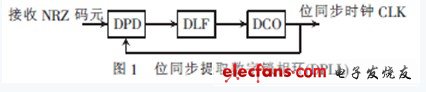
(1) The digital phase detector DPD (Digital Phase Ditector) compares the bit synchronization clock phase of the received symbol with the local DCO output, and outputs a digital signal reflecting the phase difference.
(2) Digital loop filter DLF (Digital Loop Filter) filters the phase error digital signal of the DPD output, removes the influence of random noise, and outputs a more accurate phase error digital signal.
(3) Digitally controlled oscillator DCO (Digital Controlled Oscillator) is an oscillator composed of digital circuits. It outputs a bit synchronous clock CLK of the same rate as the received symbol. Its phase is controlled by the phase error digital signal to advance or delay, and finally receive Symbol phase lock.
DPD and DCO are essential components of a digital phase-locked loop, and DLF can be added as needed. Each of the three components consists of a plurality of types of circuits that form different digital phase locked loops. The most typical digital phase-locked loop is a lead-lag digital phase-locked loop, also known as a differential rectification digital phase-locked loop, which can be realized by the single-chip microcomputer system shown in Fig. 2 when the code rate is not high. In the figure, the edge detection is also called zero-crossing detection. After it amplifies and shapes the input data signal DK1, it converts its transition edge (the zero-crossing point before shaping) into a narrow pulse ZCD and sends it to the external interrupt input terminal INT1 of the MCU. . The delay circuit in edge detection can be implemented with several levels of gates. The differential rectifier circuit has the same function as the edge detection circuit.
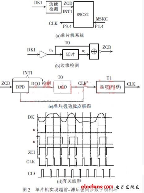
The digital phase locked loop does not use DLF. The T0 timer and its interrupt service program in the MCU implement the DCO function. When there is no transition edge of DK1 (no ZCD negative pulse), the MCU does not enter the INT1 interrupt service routine, and T0 timing is the input code period Tb. When DK1 has a transition edge, enter the INT1 interrupt service routine, first read the current value of T0 and the expected value (Tb/2 time constant), and determine whether the phase relationship between the DCO phase and the DK1 data transition edge is advanced or delayed by comparison. This adjusts the DCO phase. If the DCO phase leads, set T0 next week timing to Tb+δ to delay the DCO phase; if the DCO phase lags, set T0 next week timing to Tb-δ, make DCO phase advance, and finally realize DCO phase and DK1 data phase. locking. In short, the INT1 interrupt service routine implements DPD and DCO control functions, and the T0 timer and its interrupt service routine implement DCO functions. The T1 timer and its interrupt service routine implement a delay or phase shift, so that the phase difference between the last output bit synchronous clock CLK and DK1 (or DK2) is 0 or 180°: when the transmission system band is not limited, MSK/FSK is used. In the modulation and demodulation mode, DK1 is a square wave, and the receiving end uses integral/sampling/decision to detect. The phase difference between the two should be 0, that is, CLK is aligned with the edge of DK1 data. When the transmission system is limited in frequency band, GMSK/GFSK modulation is adopted. In the demodulation mode, DK2 (the signal after DK1 via LPF) is a bell pulse, and CLK should be aligned with the midpoint sampling/decision of DK2 symbol. The phase difference between the two is 180° or Tb/2, as shown in Figure 2(d). Show. The T1 delay is controlled by the P1.4 input signal MSKC. The INT1, T0 and T1 interrupt service block diagrams are shown in Figure 3. The main program completes the three interrupt source initializations and other initialization steps.
NINGBO SANCO ELECTRONICS CO., LTD. , https://www.sancobuzzer.com