
Car inverter circuit diagram and fault repair experience. The main indicators of the common models of car inverter products on the market input voltage: DC 10V ~ 14.5V; output voltage: AC 200V ~ 220V ± 10%; output frequency: 50Hz ± 5%; Output power: 70W ~ 150W; conversion efficiency: greater than 85%; inverter operating frequency: 30kHz ~ 50kHz.
The circuit diagram and working principle of the two common car inverter products currently have the largest sales volume on the market, and the output power of the most common car inverter is 70W-150W. The pulse width of the inverter circuit mainly adopts TL494 or KA7500 chip. Modulation circuit. A schematic diagram of one of the most common car inverter circuits is shown in Figure 1.
This article refers to the address: http://
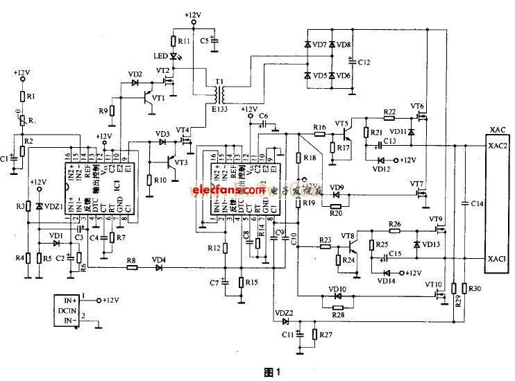
The whole circuit of the vehicle inverter can be roughly divided into two parts. Each part uses a TL494 or KA7500 chip to form a control circuit. The first part of the circuit is to provide 12V DC power from the car battery, through high frequency PWM. (Pulse-width modulation) switching power supply technology is converted into AC power of 30kHz-50kHz, 220V; the second part of the circuit is to use bridge rectification, filtering, pulse width modulation and switching power output technology, 30kHz ~ 50kHz, 220V The left and right AC power is converted into 50 Hz, 220 V AC power.
1. In-vehicle inverter circuit working principle In the circuit of Figure 1, the chip IC1 and its peripheral circuits, the triode VT1, VT3, the MOS power tube VT2, VT4 and the transformer T1 form a 12V DC conversion to 220V/50kHz AC inverter circuit. It is composed of chip IC2 and its peripheral circuits, transistor VT5, VT8, MOS power tube VT6, VT7, VT9, VT10 and 220V/50kHz rectification, filter circuit VD5-VD8, C12, etc. 220V/50kHz high frequency AC conversion to 220V/50Hz The power frequency AC conversion circuit finally outputs 220V / 50Hz AC power through the XAC socket for various portable appliances.
In Figure 1, IC1 and IC2 use the TL494CN (or KA7500C) chip to form the core control circuit of the vehicle inverter. TL494CN is a dedicated double-ended switching power supply control chip. Its suffix letter CN indicates that the package shape of the chip is a double-in-line plastic package structure. The operating temperature range is 0°C-70°C, and the limit working power supply voltage is 7V~40V. The maximum operating frequency is 300kHz.
The TL494 has a built-in 5V reference with a regulation accuracy of 5 V ± 5% and a load capacity of 10 mA. It is output through 14 pins for external circuitry. The TL494 also has two NPN power output tubes that provide 500mA drive capability. The internal circuit of the TL494 chip is shown in Figure 2. 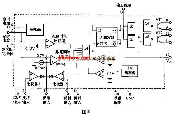
In the circuit of Fig. 1, R1 and C1 of the 15-pin peripheral circuit of IC1 constitute a power-on soft-start circuit. At the time of power-on, the voltage across the capacitor C1 is gradually increased from 0V. Only when the voltage across C1 reaches 5V or more, the pulse width modulation circuit inside IC1 is allowed to start working. When the power is turned off, C1 is discharged through the resistor R2 to ensure that the soft start circuit works normally at the next power-on.
R1, Rt, and R2 of IC15's 15-pin peripheral circuit form an overheat protection circuit. Rt is a positive temperature coefficient thermistor. The room temperature resistance value can be selected from 150 Ω to 300 Ω. Appropriate selection can improve the overheat protection circuit. Sensitivity.
When the thermistor Rt is installed, it should be tightly attached to the metal heat sink of the MOS power switch tube VT2 or VT4, so as to ensure the overheat protection function of the circuit is effective.
The voltage value U of the 15 pin of IC1 is a relatively important parameter. In the circuit of Fig. 1, U≈Vcc×R2÷(R1+Rt+R2)V, the calculated value at room temperature is U≈6.2V. As can be seen from Fig. 1 and Fig. 2, under normal working conditions, the voltage of pin 15 of IC1 should be slightly higher than the voltage of pin 16 (5V connected with pin 14 of the chip), and the voltage value of 6.2V at room temperature meets the requirements, and Leave a certain amount of margin.
When the circuit works abnormally, the temperature rise of the MOS power transistor VT2 or VT4 is greatly increased, and the resistance of the thermistor Rt exceeds about 4kΩ, the output of the internal comparator 1 of IC1 will be turned from the low level to the high level, and the IC1 pin 3 It also flips to a high state, causing the output of the PWM comparator, OR gate, and NOR gate inside the chip to flip, and the output transistor VT1 and the transistor VT2 are turned off. When the two power output tubes in IC1 are turned off, VT1 and VT3 in the circuit of Figure 1 will be saturated and turned on due to the base being at a low level. After VT1 and VT3 are turned on, the power transistors VT2 and VT4 will be insensitive due to the gate. The bias voltage is in the off state, and the inverter power supply circuit stops operating.
VDZ1, R5, VD1, C2, and R6 of IC1's 1-pin peripheral circuit form a 12V input power supply overvoltage protection circuit. The regulation value of the voltage regulator VDZ1 determines the startup threshold voltage value of the protection circuit. VD1, C2, and R6 are also composed. The protection state maintenance circuit, as long as an instantaneous input power supply overvoltage occurs, the protection circuit is activated and maintained for a period of time to ensure the safety of the power supply tube of the latter stage. Considering the normal variation of the battery voltage during driving, it is usually appropriate to select the voltage regulator VDZ1 as 15V or 16V.
C3 and R5 of the 3-pin peripheral circuit of IC1 are the key circuits that constitute the power-on soft-start time maintenance and the circuit protection state maintenance. In fact, whether it is the control of the soft start of the circuit or the start control of the protection circuit, the final result is reflected in IC1's 3-pin level state. When the circuit is powered up or the protection circuit is activated, pin 3 of IC1 is high. When IC1's 3 pin is high, capacitor C3 will be charged. After the incentive to start the protection circuit disappears, C3 discharges through R5, and the protection time of the circuit is maintained for a while due to the long time required for the discharge.
When IC1's 3 pin is high, capacitor C7 will be charged along R8 and VD4, and the voltage across capacitor C7 will be supplied to pin 4 of IC2, so that pin 4 of IC2 is kept high. It can be seen from the internal circuit of the chip of Fig. 2 that when the 4-pin is at a high level, the potential of the non-inverting input of the dead time comparator in the chip is raised, so that the output of the comparator is kept at a constant high level, via the OR gate. After the "NOR" gate, the built-in transistor VT1 and the transistor VT2 are both turned off. In the circuit of Fig. 1, VT5 and VT8 are in a saturated conduction state, and the MOS transistors VT6 and VT9 in the subsequent stage are all turned off due to the fact that the gate has no positive bias, and the inverter power supply circuit stops working.
IC1's 5-pin external capacitor C4 (472) and 6-pin external resistor R7 (4k3) are the timing components of the pulse width modulator. The determined pulse width modulation frequency is fosc=1.1÷ (0.0047×4.3) kHz≈50kHz. That is, the operating frequency of the triode VT1, VT2, VT3, VT4, and transformer T1 in the circuit is about 50 kHz. Therefore, the high frequency ferrite core transformer should be selected for T1, and the function of the transformer T1 is to boost the 12V pulse to a pulse of 220V. The primary number of turns is 20 × 2 and the number of secondary turns is 380.
IC5's 5-pin external capacitor C8 (104) and 6-pin external resistor R14 (220k) are the timing components of the pulse width modulator. The determined pulse width modulation frequency is fosc=1.1÷ (C8×R14)=1.1÷(0.1 ×220) kHz ≈ 50 Hz.
R29, R30, R27, C11, VDZ2 constitute the overvoltage protection circuit of the 220V output terminal of XAC socket. When the output voltage is too high, it will cause the voltage regulator VDZ2 to breakdown, so that the voltage of IC2's 4 feet goes to ground, and the protection in chip IC2 The circuit operates to cut off the output.
The MOS tubes VT2 and VT4 in the vehicle inverter circuit have a certain power consumption, and heat sinks must be added. Other devices do not need to install heat sinks. When the car inverter product is continuously used in high power applications, a small 12V fan should be installed inside to help dissipate heat.
2. Component parameters in the circuit
The parameters of each component in the circuit are listed in the attached table. 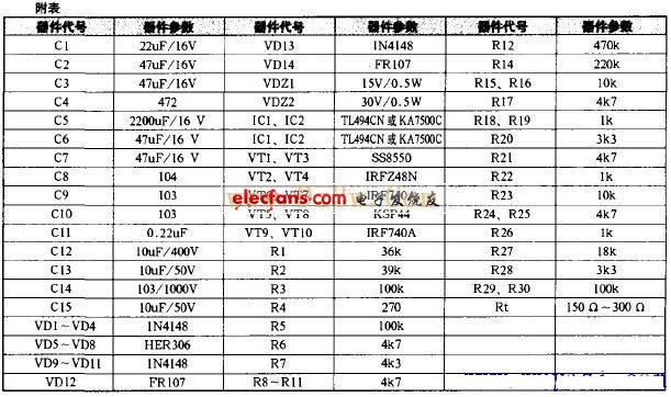 3. Maintenance points of the car inverter products Since the car inverter circuit generally has a power-on soft-start function, it will wait for 5s-30s after the power is turned on, and then there will be an output of 220V AC, and the LED indicator points. bright. When the LED indicator is off, it indicates that the inverter circuit is not working.
When the power is turned on for more than 30s and the LED indicator is not lit, you need to measure the AC voltage at the XAC output socket. If the voltage is about 220V, it means that only the LED part of the circuit appears. Fault; if the AC voltage value measured at the XAC output socket is 0, the fault is caused by the inverter circuit in the front stage of the inverter not working, and the protection circuit inside the chip IC1 may have started.
The method for judging whether the internal protection circuit of the chip IC1 is activated is: using the DC voltage of the multimeter to measure the DC voltage value of the 3-pin to ground of the chip IC1. If the voltage is above 1V, the protection circuit inside the chip has been started, otherwise the fault is indicated. The reason is caused by the action of the non-protection circuit.
If the voltage of the pin 3 of the chip IC1 is above 1V, indicating that the protection circuit inside the chip has been started, it is necessary to further test the DC voltage between the pins 15 and 16 of the chip IC1 with the DC voltage of the multimeter, and the IC1 of the chip IC1. DC voltage between 1, 2 feet. Under normal circumstances, the DC voltage of pin 15 to ground of IC1 in the circuit of Figure 1 should be higher than the DC voltage of 16 feet to ground. The DC voltage of 2 feet to ground should be higher than the DC voltage of 1 pin to ground, only when these two When the condition is satisfied at the same time, the DC voltage of the 3-pin to ground of the IC1 of the chip can be about 0V, and the inverter circuit can work normally. If it is found that a test voltage does not satisfy the above relationship, it is only necessary to find the cause of the fault by pressing the corresponding branch to solve the problem.
4. Main components and parameters of the car inverter products and replacement Figure 1 The main components in the circuit are the drive tube SS8550, KSP44, MOS power switch tube IRFZ48N, IRF740A, fast recovery rectifier diode HER306 and PWM control chip TL494CN (or KA7500C ).
The SS8550 is a PNP type triode in the form of a TO-92 package. The pin electrode is identified by the way that when facing the printed surface of the transistor, pin 1 is the emitter E, 2 is the base B, and 3 is the collector C.
The main parameters of SS8550 are: BVCBO=-40V, BVCEO=-25V, VCE(S)=-0.28V, VBE(ON)=-0.66V, fT=200MHz, ICM=1.5A, PCM=1W, TJ= 150 ° C, hFE = 85 ~ 160 (B), 120 ~ 200 (C), 160 ~ 300 (D).
The surface mount device model corresponding to the SS8550 in the TO-92 form package is the S8550LT1, which is packaged in the form of SOT-23.
SS8550 is a relatively common and easy-to-buy triode on the market, and the price is relatively cheap. The price is only about 0.3 yuan.
The KSP44 is an NPN type triode in the form of a TO-92 package. The pin electrode is identified by a method in which the pin 1 is an emitter E, 2 is a base B, and 3 is a collector C when facing the printed surface of the triode.
The main parameters of KSP44 are: BVCBO=500V, BVCEO=400V, VCE(S)=0.5V, VBE(ON)=0.75V, ICM=300mA, PCM=0.625W, TJ=150°C, hFE=40~200 .
KSP44 is a high-voltage triode commonly used in telephones. When the KSP44 is damaged and cannot be purchased, it can be replaced by the commonly used triode KSE13001 in the fluorescent lamp circuit. KSE13001 is a product of FAIRCHILD. The main parameters are BVCBO=400V, BVCEO=400V, ICM=100mA, PCM=0.6W, hFE=40~80. Although the package form of the KSE13001 is also TO-92, the order of the pin electrodes is different from that of the KSP44. This should be paid special attention when replacing. The KSE13001 pin electrode is identified by the fact that when facing the printed surface of the triode, the pin electrode 1 is the base B, 2 is the collector C, and the emitter E is the emitter E.
The IRFZ48N is an N-channel enhancement MOS fast power switch in the form of a TO-220 package. The pin electrode sort 1 is the gate G, 2 is the drain D, and 3 is the source S. The main parameters of IRFZ48N are: VDss=55V, ID=66A, Ptot=140W, TJ=175°C, RDS(ON)≤16mΩ.
When the IRFZ48N is damaged and cannot be purchased, the N-channel enhancement type MOS switch tube IRF3205 with the same package type and pin electrode ordering can be replaced. The main parameters of IRF3205 are VDss=55V, ID=110A, and RDS(ON)≤8mΩ. Its market price is only about 3 yuan per piece.
The IRF740A is an N-channel enhancement MOS fast power switch tube in the TO-220 form package. The pin electrode sort 1 is the gate G, 2 is the drain D, and 3 is the source S.
The main parameters of IRF740A are: VDSS=400V, ID=10A, Ptot=120W, RDS(ON)≤550mΩ.
When the IRF740A is damaged and cannot be purchased, it can be replaced by an N-channel enhancement type MOS switch tube IRF740B, IRF740 or IRF730 in the same package type as the pin electrode. The main parameters of the IRF740 and IRF740B are identical to those of the IRF740A. The main parameters of IRF730 are VDSS=400V, ID=5.5A, and RDS(ON)≤1Ω. Although the parameters of IRF730 are slightly worse than those of IRF740 series, the parameters of inverters with power below 150W are more than enough.
The HER306 is a fast recovery rectifier diode of 3A and 600V. Its reverse recovery time is Trr=100ns. It can be replaced by HER307 (3A, 800V) or HER308 (3A, 1000V). For automotive inverters with powers below 150W, the quick recovery diode HER306 can be replaced with BYV26C or the most easily purchased FR107. BYV26C is a fast recovery rectifier diode of 1A, 600V, its reverse recovery time is Trr=30ns; FR107 is 1A, 1000V fast recovery rectifier diode, its reverse recovery time = 100ns. Considering the parameter of the reverse recovery time of the device, it is more suitable to use BYV26C for substitution.
The TL494CN and KA7500C are PWM control chips. Analysis of various on-board inverter products on the market can be found that some TL494CN chips are used in some car inverter products, some use two KA7500C chips, and some use one for each of the two chips. What's even more bizarre is that some products are actually confusing, and the logo of one of the TL494CN or KA7500C chips is polished, and then labeled with various weird chip models, which makes the maintenance staff feel confused. In fact, as long as you look at the peripheral circuit of the chip, you know that the chip used must be TL494CN or KA7500C.
After carefully reviewing and comparing the original pdf data of the TL494CN and KA7500C chips, it is found that the external pins of the two chips are exactly the same, and even the internal circuits are almost identical. The difference is only the internal operation of the two chips. The size of the reference source on the input side is slightly different, and has no effect on the function and performance of the circuit. Therefore, the two chips can be used interchangeably, and the parameters of the peripheral circuit of the chip need not be modified. The experience of successful replacement in the actual use process also confirmed the feasibility of this substitution and the reliability of the circuit performance after replacement.
Since it is difficult to find the KA7500C chip on the market, and even if it can be bought, its price is at least twice that of the TL494CN chip. Therefore, the successful experience and method of directly substituting the KA7500C chip using TL494CN is introduced here. It is indeed a good news for manufacturers of transformer products and maintenance personnel.
Safety Light Curtain,Safety Curtain,Laser Safety Light Curtain,Safety Optic Light Curtain,Security Light Curtain,Press Brake Safety Light Curtains
Jining KeLi Photoelectronic Industrial Co.,Ltd , https://www.sdkelien.com