
1 Introduction
Due to the increasingly serious energy crisis in the world, light-emitting diodes (LEDs) have been highly valued as a high-efficiency light source. Not only white light LEDs have been widely used in backlights such as mobile phones, PDAs, and LCD TVs in consumer electronics. Traffic signal signs, industrial communication lighting systems, automotive lighting and large-scale general industrial and civil lighting fields will also be widely used. As a light source, the advantages of LED are mainly reflected in three aspects: energy saving, environmental protection and longevity and durability. First of all, the energy consumption of LED is theoretically only 10% of incandescent lamps and 50% of fluorescent lamps. In terms of service life, LEDs use solid light, which is shock-resistant, impact-resistant and not easily broken. The life expectancy can reach 100,000 hours. In terms of environmental protection, waste is recyclable and non-polluting because it does not use easy pollutants such as mercury in the production process.
One of the key technologies in LED applications is to provide power or drive circuits that are compatible with their characteristics. In lighting applications, today's high-brightness white LEDs operate at currents of up to 150mA to 3A and turn-on voltage drops of up to 3~5V to provide higher brightness. Due to the increase of power, the traditional resistor current limiting, linear regulation, and the efficiency of the charge pump driving method can not be further improved by the principle. The PWM switching power supply type DC converter becomes the preferred LED driving solution. This paper proposes a chip for the controller of the boost LED driver circuit. Considering that the LED is a typical current-type device, the fluctuation of current will affect its luminous efficiency and color, and the current exceeding the rated value will impair its life and reliability. . Therefore, current mode control has significant advantages in LED driving. Moreover, the PWM control technology has been developed so far, and its current control mode has also developed various modes. Compared with the loop design with more complicated average current control mode and hysteresis current control mode with more electromagnetic interference problems, the peak current control mode loop design is simpler and can effectively limit the current.
Taking into account the above factors, the chip uses a peak current control mode in the design, and integrates a slope compensation circuit to make it have a wide voltage operating range (3~16V). This paper first gives the modeling and loop compensation design of the entire control system. Next, for the LED dimming requirements, the digital dimming function module is designed based on the traditional peak current mode controller module. The third part introduces the control function circuit of the non-sampling resistor in the chip, which realizes the sampling current by directly sampling the drain-source voltage of the power switch tube, that is, Rds(on) sampling, which reduces the loss on the sampling resistor and can effectively improve the system. s efficiency. Finally, the system structure, layout and test results of the control chip are given.
2 system modeling and loop compensation design
The step-up LED driver circuit and control loop diagram are shown in Figure 1. The load LED current input voltage error amplifier (EA) is sampled by the resistor Rs1, the output of the error amplifier is passed through the compensation network output as the reference of the current peak comparator, and the current of the resistor Rs2 is sampled on the positive side of the comparator S1, and the Ramp is the peak value. The slope compensation current in current control. The clock signal CLK determines the switching frequency and the opening of the switching tube. When the current signal is greater than the set threshold, the output of the comparator becomes high, and the logic circuit flips the switching tube to turn off.
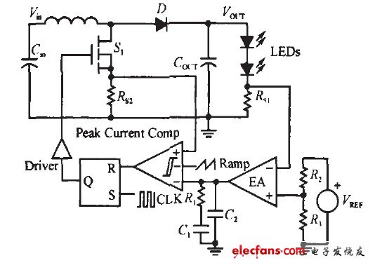
Figure 1 Step-up LED driver circuit control chart
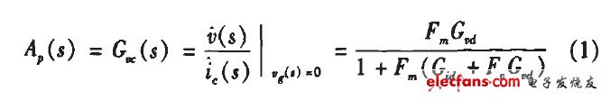
A small signal model circuit as shown in Figure 2 can be established. For the boost type power stage circuit, two important transfer functions Gvd(s) and Gid(s) of the original power level can be obtained by using the state space averaging method, and the output voltage can be derived from the command current signal according to the model in the figure. Effect power level transmission letter Ap(s).
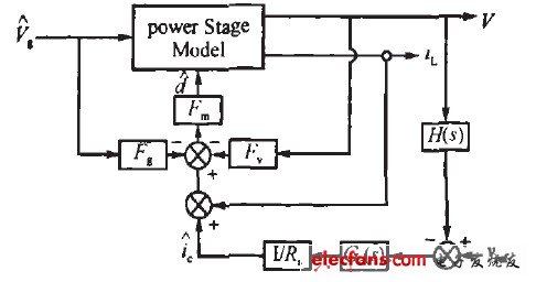
Figure 2 Peak current mode control small signal model
Where Fm=1/MaTs, Fv=D'2Ts/2L, Ma is the slope of the slope compensation current, L is the filter inductance, Ts is the switching period, and D is the steady-state duty. Consider the transfer function T(s) of the entire loop;
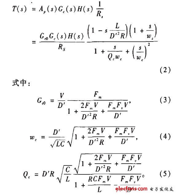
The phase-frequency curve of the loop transmission before compensation is shown in Fig. 3. The system has two poles (p1, p2), a zero point z of the left half plane (caused by the output Capacitor ESR), and a zero point z1 of the right half plane. It should be pointed out that if there is no introduction of the current feedback control system with the slope compensation circuit, the output LCR network determines that the loop system is a high Q value system, and the current feedback makes the Q value of the system greatly reduced, but The zero point in the right half plane increases the crossing frequency and makes the phase margin worse. The compensation method that can be used is to add a single zero-point single-pole compensation network as shown in Figure 3. The Gc(s) expression is
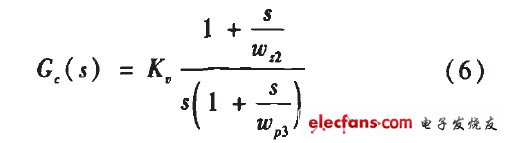
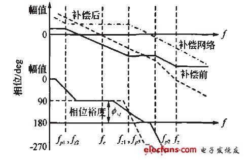
Figure 3: Open loop frequency response of the system before and after compensation
Where z2 is used to compensate the pole p1, the pole of the coordinate origin can increase the loop gain of the low frequency with a small DC steady state error, p3 cancels the amplitude increase brought by z1, suppresses the noise close to the open frequency, and the final crossing frequency fc is set. Set at about 1/10 of the switching frequency. The simplest compensation method can also use a single-pole compensation network. To ensure the phase margin, the shortcoming is that the bandwidth of the loop will be smaller and the dynamic response of the system will be slower. For the actual application of the step-up LED driver circuit and the simulation results in MATLAB (as shown in Figure 4), from the simulation results, the loop is near the crossing frequency under the design of the ramp current and compensation network. The phase margin is greater than 45°, and the system is stable, which is basically consistent with the results of the formula calculation.
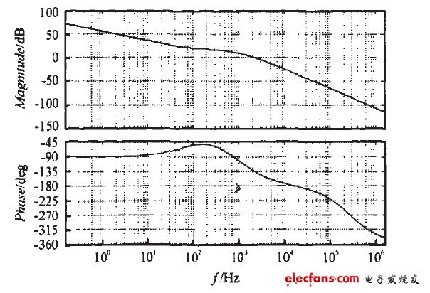
Figure 4 MATLAB simulation results
Our company is specialized in supplying high quality Brass Fitting including,nuts,union,connector,elbow,tee,distributor,adapter,other Copper/Brass Products like Copper Tube ,air conditioner valve,sight glass,hand valve, Access Valve , Filter Drier ,Solenoid Valve,Capillary Tube and so on. Standard can be according to customers` requirement, we can provide you all kings of standards.The structure and dimension of each fitting is customizable, ensuring customers are getting the right fitting for their needs.Our parts have been exported to over 50 countries all over the world.
Brass Fitting
Refrigeration Ball Valve,Brass Hose Fitting,Air Conditioner Ball Valve,Ball Valve With Charging Port
ZHEJIANG ICE LOONG ENVIRONMENTAL SCI-TECH CO.,LTD. , https://www.ice-loong.com