
With the development of computer technology, semiconductor technology and electronic technology, embedded systems are widely used in industrial manufacturing, process control, communication, instrumentation, instrumentation, etc. due to their small size, high reliability, low power consumption, and high integration of software and hardware. Automobiles, ships, aviation, aerospace, military equipment, consumer products and many other fields. Embedded system hardware design and debugging is the basis for successful embedded system design, and the design and debugging of power circuit in hardware circuit is the key to successful system hardware debugging. This paper starts from the practical application, combined with some problems encountered in the design and debugging process of the embedded system power supply in the welding machine control system, analyzes and discusses the design and debugging method of the embedded system power supply.
1 system hardware structure
In the design of welding machine control system based on embedded system, AT91RM9200 is used as the core microprocessor of the system. SDRAM, SRAM and Flash are expanded according to the requirements of the control system. The keyboard and liquid crystal display circuit can adjust and display the real-time parameters in real time. When the alarm occurs, the RS485 serial interface completes the data transmission communication and can perform infrared remote control operation. The system hardware structure is shown in Figure 1.

Figure 1 system hardware block diagram
2 system power supply design
2.1 System power supply working principle
The AT91RM9200 is a system chip built entirely around the ARM920T processor. It has a rich system and application peripherals and standard interfaces, making it a low-power, low-cost embedded industrial grade product. The AT91RM9200 provides a full-featured power management controller (PMC) that optimizes overall system power consumption and supports normal, idle, slow clock, and Standby modes of operation, providing different power levels and event response delay times [1]. In Idle mode, the ARM processor clock is disabled and waits for the next interrupt (or master reset); the slow clock mode is the mode selected after reset, in which the main oscillator and PLL are turned off to reduce power consumption; Standby mode is slow The combination of clock mode and idle mode enables the processor to respond quickly to wake-up events while maintaining low power consumption. When the system works normally, it is powered by the external DC power supply and charges the battery. When the external power supply is disconnected, it automatically switches to the internal backup battery.
2.2 Power circuit design
The AT91RM9200 has five types of power supply pins: the VDDCORE pin is used to supply power to the core, typically 1.8 V. VDDPLL and VDDOSC supply power to the PLL or oscillator, typically 1.8 V. VDDIOP and VDDIOM are used to provide peripheral I. /O line, USB transceiver and external bus interface I / O line power supply, usually 3.3 V. In addition, the system's keyboard and display circuit supply voltage requires +5 V power supply. Therefore, this control system requires three sets of power supplies. By analyzing the control requirements and performance of the entire control system, it is determined that the load current of the system is about 3 A. Therefore, the regulator of the system power supply uses ON's LM2576 series regulator to regulate the external DC power supply to the +3.3 V and +5 V power supplies required by the system. Since the system core power supply requires 1.8 V, the system should use a secondary power conversion circuit. This article selects TI's micro-power, very low-dropout PMOS regulator (LDO chip) TPS72518 as the core power conversion chip, and regulates +3.3 V to +1.8 V to provide working power for the processor core. The system power supply circuit is shown in Figure 2. Figure 2 shows the PCB design method for embedded system power supply decoupling. C3 and C6 are electrolytic bypass capacitors of the voltage regulator chip. They can be connected to the circuit to make the circuit work stably. C2, C5 and C8 are output stable capacitors for reducing output ripple, output noise and load current. The effect has a good effect. According to the working requirements of the regulator itself, the capacitors are respectively selected as electrolytic capacitors of 10 μF and 100 μF.
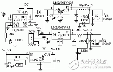
Figure 2 system power circuit diagram
The performance of embedded systems based on 32-bit microprocessors depends to a large extent on the stability and reliability of the clock circuit, and the stability of the clock circuit depends mainly on the stability of the system phase-locked loop (PLL). Therefore, in the PLL analog part of the power supply should use a filter circuit to ensure the stability of the power supply [2]. The parameters of the key components of the microprocessor's internal clock, power supply, and reset control play an important and even decisive role in the various modes of operation of the system. Therefore, in order to ensure that the parameters set in various operating modes are unchanged, the power supply circuit of the backup battery is usually provided in the embedded system design. As shown in Figure 2, TI's battery charger BQ24200 is used as the backup battery of the system power supply. When the system is working normally, the external power supply charges it. After the external power supply is cut off, it supplies system power, so that the system can save important parameters.
3 system power supply debugging
3.1 Debugging content and steps
A relatively large embedded system hardware circuit, should be divided into modules for welding, debugging, to avoid problems when not encountered. Since each circuit module in the system needs to be connected to the input power supply, if the power input is improper, the output result will be incorrect or even the integrated circuit will be burned out. Therefore, the system power supply module should be installed and debugged first. The successful debugging of the system power circuit module is the key to the successful debugging of the entire hardware circuit.
After soldering the components according to the circuit diagram, carefully check whether the components are soldered incorrectly, whether there is any solder joint or short circuit of the solder slag, and perform power-on debugging after checking. The output power of the DC stabilized power generator is connected to the input port (POW1) of the system power module. The input power Vin is adjusted to +6 V. Use the oscilloscope to check the 1.8 V, 3.3 V, and 5 V output ports of the system power supply. There is no voltage output. The power was re-examined and the electrolytic capacitor C6 was burned black because the positive and negative polarities of C6 were reversed. After the new capacitor is soldered correctly, the power-on debugging is performed. The 1.8 V and 5 V voltage output terminals are normal, and the 3.3 V voltage output terminal voltage is less than 3 V. After viewing the data sheet of the regulator chip LM2576, adjust the input power supply Vin and simultaneously detect the voltage values ​​of the three sets of system power supplies. When the three sets of power supply outputs are correct, the input voltage Vin is about 6.7 V. Since the load current of this control system is about 3 A, a load resistor with a load current of 3 A is added to the circuit to test the stability of the system power supply. After debugging, the components such as capacitors and inductors heat up normally and the output voltage value is correct. At this point, the system power module is successfully debugged.
Next, install and debug other module circuits step by step. Power-on detection is performed every time a module is installed, mainly detecting the system power supply voltage and the input voltage of the module, and whether the output result is correct. When the whole system hardware circuit is installed and power-on debugging, it is found that the system power supply is unstable, that is, the DC stabilized input power source often loses power, causing the system power supply to work abnormally. Due to the large number of system circuits, the inspection is difficult and the problem has not been solved. After several power-on detections and debugging, it was found that a voltage (boost) converter in the circuit smoked - the chip was burnt. Careful inspection of the chip's data sheet, found that the chip model is wrong, the positive and negative feedback voltage pins are reversed. After the chip is removed, the system power supply is working properly.
3.2 Analysis of debugging results
The system power supply debugging and the installation and debugging process of the whole system hardware circuit are analyzed. Combined with the problems encountered during the installation and debugging process, the following conclusions are drawn:
1 Chip resistors and capacitors are mostly made of ceramic material that is easily broken by collision. The chip-type integrated circuit has many pins, narrow pitch and low hardness, which can easily lead to short-circuit soldering and soldering. Therefore, you should master the techniques of temperature control, preheating, and light touch during disassembly and welding.
2 Before commissioning the power module, you must carefully check whether the components are installed incorrectly. Use a voltmeter to check whether the circuit has a virtual solder or a short circuit of the slag to ensure the correctness of the circuit and avoid burning the components.
3 If there is not much confidence in power-on, consider using an adjustable regulated power supply with current limiting function to slowly increase the voltage value of the regulated power supply, and detect the input current (voltage) and output voltage until the output voltage is satisfied. Claim.
4 When debugging a relatively large system circuit, you should first install and debug the system power supply. After the debugging is successful, install and debug other modules step by step. Power up the test every time one module is installed, and then debug another module after making sure it is correct.
Conclusion
This paper takes the embedded control system based on AT91RM9200 as an example. It focuses on the design ideas and methods of the system power supply circuit, as well as the installation and debugging process of the system power supply. Combined with the problems encountered during the debugging process, the debugging method and attention of the embedded system circuit. The matter was analyzed. With the wide application of embedded systems, the design and debugging of power supply circuits is especially important. The design and debugging ideas of this paper are worth learning.
Doorbell speaker:
Doorbell speaker is a kind of micro speaker unit which uses a diaphragm made of Mylar material. Doorbell speakers are of ultrathin design and lightweight and clear voice. It is widely used in building security industry (e.g. intercom, video door phone, intelligent door control..)
There are two types of Mylar speakers from the shapes:
1) Round shapes, we have products from 10mm to 57mm in diameter.
2) Oblong shape, we have products in sizes of 1510/1712/1813-..


FAQ
Q1. What is the MOQ?
XDEC: 2000pcs for one model.
Q2. What is the delivery lead time?
XDEC: 15 days for normal orders, 10 days for urgent orders.
Q3. What are the payment methods?
XDEC: T/T, PayPal, Western Union, Money Gram.
Q4. Can you offer samples for testing?
XDEC: Yes, we offer free samples.
Q5. How soon can you send samples?
XDEC: We can send samples in 3-5 days.
Doorbell Speaker,Doorphone Speaker,Video Doorphone Speaker,Doorbell Wireless Speakers
Shenzhen Xuanda Electronics Co., Ltd. , https://www.xdecspeaker.com