
In recent years, the application of light-emitting diodes (LEDs) has been growing, covering a wide range of markets, including automotive lighting applications such as indicator lights, spotlights and headlights, camera functions such as display backlights and camera flashes. Consumer products such as LED display backlights and projection systems, architectural features such as architectural lighting and signs, and many other applications. The LED has high brightness, high luminous efficiency and fast response. Incandescent lamps have been replaced in many ways due to their low energy consumption, long service life, low heat release and the ability to emit colored light.
As the efficiency of LEDs continues to increase, the amount of lumens per watt that is generated continues to increase, and the use of LEDs for general illumination becomes more and more practical. For example, in 2003, a fluorescent tube equivalent to 3000 lumens required more than 1300 LEDs with an efficiency of 30 lumens per watt to achieve comparable results. However, by 2005, the number of LEDs required to achieve the same fluorescent tube illumination was reduced by a factor of 20, requiring only about 50, each LED having a luminous efficiency of 50 lm/W or higher and a luminous intensity of 60 lumens.
LED lighting level
There are four links in LED production, or four areas. The first link is called product link 0, which refers to the production device itself. The second link of product link 1 is the first-level package, which refers to the method of connecting the device to the power supply through chip bonding and wire bonding to form a surface mount package. The third link of product link 2 refers to the secondary package. Put multiple primary packages together to create the light output required for an external signal or outdoor lighting application. The fourth link, product link 3, is to systematically package the entire system or solution.
The primary LED package includes a single LED and a complex LED matrix package. In a standard LED array, each LED is connected to a substrate electrode. LEDs can be handled separately or connected together. Most of this type of package utilizes epoxy adhesive chips. For high-brightness LED applications, such as outdoor lighting or tail-projection screen illumination, a matrix-structured LED is required. In this configuration, the LEDs are arranged in tight rows and columns to obtain as much light as possible. Figure 1 is a matrix diagram of LEDs that together emit a large amount of lumens. The number and alignment of the LEDs requires good thermal conductivity of the die attach material to keep the LEDs as cold as possible.
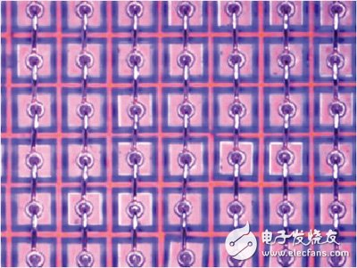
Figure 1 LED matrix diagram
Matrix LED packages are the basis for many systems in production. Their recent popularity is due to the fact that this structure can get more lumens per watt of power. However, matrix LED packages pose significant challenges for chip bonding and wire bonding compared to single-chip packages. High-brightness LED applications require maximum heat transfer to meet performance requirements.
Package high brightness LED
Matrix LED process steps include material preparation, chip pick and place, pulse reflow, cleaning, wire bonding, and testing. The following discussion will focus on pulse reflow (low temperature eutectic bonding) and wire bonding steps. An example is a 98 290 祄 LED matrix using AuSn bonding. The LEDs are electrically connected together in the column direction. The goal is to connect the LEDs to the substrate using metallurgical eutectic interconnects, placing the LEDs as close as possible based on component tolerances (a gap of about 1 mil). Figure 2 shows the 290-inch LED matrix.
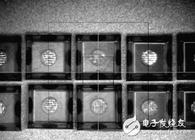
Figure 2 Attaching a 290 micron LED to the AuSn before wire bonding
Pulse reflow
The key to the LED packaging process is to avoid holes in the eutectic solder of the diode and its substrate, and the thermal and electrical connections required to produce stable light transmission are accomplished by solder. The eutectic chip adhesive transfers the enormous thermal energy generated by the diode to maintain the thermal stability of the device. Controlling the eutectic bonding process is the key to achieving high yield and reliability.
Accurate eutectic component bonding includes diode pick-and-place, on-site reflow of pre- or pre-tinted devices using programmable x, y or z-axis agitation, as well as programmable pulse heating or steady-state temperatures. To achieve an optimized heat transfer solder interface, the temperature profile of the bonding process must be repeatable with the ability to increase at high temperatures. When the interface temperature rises to the appropriate eutectic temperature, the heating mechanism must be maintained at the set temperature and the temperature overshoot should be as small as possible. After a necessary reflow time, the heating mechanism must be able to control the cooling, so that the damage to the diode is as small as possible, so that the eutectic material can reach the metallurgical balance. This balance is achieved by applying both active thermoelectric pulse heating and cooling gas.
LED matrix packages are temperature-sensitive processes that require careful control during the packaging process. The reflow profile of the in-situ eutectic die bonding process is designed to provide a constant melt and non-porous bonding interface. This is necessary to keep heat out of the diode and to maintain temperature stability while the LED is operating.
This example uses a wire to reinforce the pulsed heat return. During the pulse heating cycle, a rising curve controlled by a servo system causes the temperature to rise from the preheating temperature to the reflow temperature, which is a lower temperature over conventional heating systems. The repeatability of the temperature profile is critical to the process, allowing for proper eutectic infiltration with minimal voids and no damage to the LED. The required temperature profile depends on the materials used for the substrate, the size of the substrate, and the composition of the solder. Infiltrate with a programmable curve with just a click to form a temperature command curve. The system captures the actual temperature profile during wire bonding and has process traceability. The pulse heating curve control allows the LED matrix to be batch reflowed, reducing overall cycle time and keeping the high temperature time as low as possible, protecting temperature sensitive LED devices.
Wire bonding
After bonding the LEDs, the interconnections are completed using bond wires. High-density, high-frequency LED matrix formats require LEDs to be interconnected using metal wires. Although there are a variety of wire bonding methods, such as ball and wedge, the test data shows that the chain solder joints using a ball bonder achieve the best results. For standard ball/pin welding, the ball is first formed and the leads are pulled to the pins to form the interconnection of the LEDs. The chain bond is a variant of the ball/pin weld, the pin is not the terminal, and the coil-pin compound is performed thereon to complete the chain wire bond set. Figure 3 shows the use of a wire bonder for chain welding, setting a ball-line arc - intermediate stitch - line arc - intermediate stitch - line arc. Finally, a line arc pin is then formed with a ball stitch on each terminal pin to ensure connection. This is not a completely new technology, but it has been further developed through material selection and software tools. Chain welding results in higher yields because it forms a standard spherical weld that does not necessarily form an airless sphere. In addition, due to the chain-shaped solder pin pattern, there is less light occlusion, and the tensile test results prove that it has better pull strength.
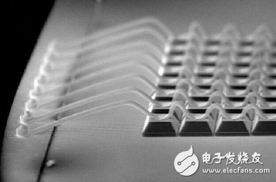
Figure 3 Chain welding with a secure connection
in conclusion
Matrix assembly of LEDs results in higher density, higher brightness LEDs. This configuration poses a challenge to the package due to the high concentration of heat and the requirement for high frequency wire bond connections. Bonding wires must be placed precisely in areas where the LEDs are dense. This connection has a stable line-arc shape and the connection strength should be strong enough to withstand mechanical shock and stress due to the large thermal disturbances. Three steps in the packaging process are critical. The first step is to take the chip with high precision to achieve a matrix LED application within the geometric tolerances of the LED. Second, it is necessary to apply pulsed heating to control the batch eutectic reflow chip bonding process for assembly production, LED protection, and better thermal conductivity while providing high quality and low risk performance. Third, the chain connection provides excellent array electrical and mechanical connections for all LEDs. These packaging processes are used to achieve high brightness, while also achieving heat dissipation and maximum light extraction efficiency.
Fiber Optical Distribution Box(Metal) Fiber Optic Distribution Box is specially designed for FTTH or FTTB for Indoor/Outdoor application. It is can manage single,ribbon & bundle fiber cables. It consists of splicing, distribution and panel with ensures the excess fiber cords and pigtails in good order, no interval and easy for management and operation. It offers mufti-functions of distribution management.

Indoor Fiber Optical Distribution Box(Metal)
Indoor Fiber Optical Distribution Box(Metal),Fiber Optic Distribution Cabinet,Metal Electrical Boxes,Metal Equipment Cabinet
Sijee Optical Communication Technology Co.,Ltd , https://www.sijee-optical.com