
Abstract: The following arTIcle describes the relaTIonship between small-signal and large-signal inputs and the noise + distorTIon performance of a data converter and its impact on the sensiTIvity and AC performance of a digital receiver system.
IntroductionWhen using a high-performance Nyquist analog-to-digital converter (ADC) in a sampling or sub-sampling receiver design, an RF designer needs to know the ADC's noise performance for both small- and large-signal inputs. The receiver must meet sensitivity and blocking (high-level interference) requirements under these two signal level extremes, and the ADC generates different amounts of noise for each of these levels, which can be expressed in terms of its effective noise figure. It is important for the user to understand the amount of ADC noise contribution in the receiver line-up when determining the ADC's AC requirements. For the following discussion, it is assumed that the noise is flat across the converter's Nyquist band.
Determining the Effective Noise FigureFor small analog input signals (on the order of -35dBFS), the thermal + quantization noise power dominate the ADC noise floor, which is used to approximate the ADC's effective noise figure (NF). Once the ADC's NF is known , the cascaded noise figure equation¹ can be used to determine the overall receiver noise figure at the receiver input terminal. The level of ADC noise contribution for small-signal inputs is used for signals near and just above the receiver sensitivity. Refer to Figure 1 and use the following steps to approximate the ADC effective noise figure for small-signal analog input levels:
Calculate the ADC's full-scale level (in dBm). This step is necessary because the thermal + quantization noise power is commonly given in units of dBFS and noise figure is calculated with respect to dBm. Determine the thermal + quantization noise floor level (in dBm) either from the component vendor's data sheet or by measurement (for a small- signal input level on the order of -35dBFS). Calculate the normalized noise floor level in 1Hz-bandwidth by subtracting 10 × log (fSAMPLE / 2) where fSAMPLE is given in units of Hz. Determine thermal noise power in 1Hz bandwidth;
KTB = 4.002 × 10⁻²¹ Watts (or in log form = -174dBm), where
K = Boltzmann's constant = 1.381 × 10⁻²³ W / Hz / K,
T = 290 K at room temperature
B = Normalized bandwidth of 1Hz Calculate the effective noise figure by subtracting the result from step 4 from the result calculated in step 3. In practice, once the ADC's effective noise figure is known, and the cascaded noise figure of the analog circuitry (RF & IF) is determined; the minimum power gain ahead of the ADC is selected to meet the required receiver noise figure. The amount of power gain places an upper limit on the maximum blocker, or highest interference level the receiver can tolerate. For cellular basestation applications , the ADC often does not have sufficient dynamic range to meet both the noise figure requirements (receiver sensitivity) and maximum blocker requirements without implementing some amount of automatic gain control (AGC). The AGC can be included either in the RF or IF stages ( or both). When higher resolution converters are used, the thermal + quantization noise is lower thereby decreasing the ADC's effective noise figure. As a result, less gain is need ed in the receiver line-up to achieve the receiver noise figure thereby reducing the need for an AGC circuit when higher-level blockers are present.
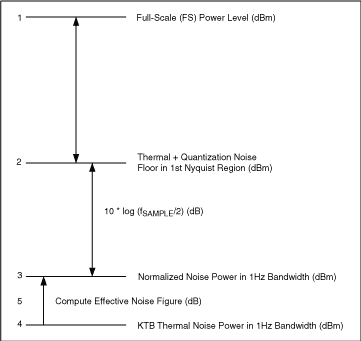
Figure 1. Determining an ADC's effective noise figure for small-signal inputs for receiver sensitivity requirements.
For intermediate signal level inputs, the converter's differential non-linearity (DNL) noise increases as major subrange boundaries are traversed. The intermediate signal levels can be defined for signal levels greater than -35dBFS, but still below those input levels where clock jitter significantly increases the ADC's noise power. Intermediate signals levels are not a major focus of this application note since they are between the sensitivity and blocking signal level extremes.
For a large-level analog input signal (closer to full-scale), the ADC noise floor level increases, mainly due to clock jitter. The ratio of the signal to noise level is defined as the signal-to-noise ratio (SNR) . The acceptable level of ADC noise power in any particular application is calculated for the case when both a blocker and smaller signal are applied to the receiver terminal simultaneously. In any application, SNR can be specified for any bandwidth, however it is usually specified either in the first Nyquist region (half the sampling rate) or in the desired signal bandwidth. It is therefore very important for the user to pay close attention to the bandwidth used throughout the calculations.
Refer to Figure 2 and follow the steps below to approximate the ADC's effective noise figure for large analog input signals: Determine the converter's full-scale level (in dBm) knowing the maximum allowable VP-P and input terminating resistance, RIN. Note the level from which SNR is either specified in the manufacturer's data sheet or measured by the user (shown as X dB in Figure 2). With SNR known, calculate the converter's noise power in the first Nyquist region (in dBm). Using the sample rate, calculate 10 × log (fSAMPLE / 2) where fSAMPLE is given in units of Hz. Determine the converter's noise power in a 1Hz bandwidth by subtracting the results obtained in (4) from the results in (3). Calculate KTB for B = 1Hz (equal to -174dBm at room temperature). Calculate the effective noise figure by subtracting the results from (6) from the results obtained in (5).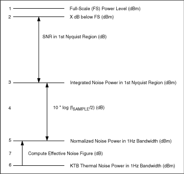
Figure 2. Determining ADC effective noise figure for large-signal inputs for receiver blocker requirements.
Numeric Example using the MAX1428The MAX1428, has the following preliminary specifications (See Table 1):
Table 1. The MAX1428 Preliminary Electrical Characteristics
The MAX1428 ADC Noise ContributionsAssume that a terminating resistance placed across the differential input pins of the MAX1428 produces a total differential resistance of 200Ω. The full-scale input level is calculated to approximately equal +6 dBm (2.5VP-P across 200Ω). For a clock rate of 80Msps, the thermal + quantization noise-floor power equals -78.3dBFS or -72.3dBm in the first Nyquist region. As the 70MHz analog input level is increased above -35dBFS, but not close to full-scale, the converter DNL noise adds 1.3dB to the total converter noise floor to -71dBm. As the input level is increased further and approaches full-scale, the noise floor increases an additional 1.3dB due to ADC clock jitter to a value of -69.7dBm resulting in an effective noise figure of 28.3dB (per procedure outlined in Figure 2).
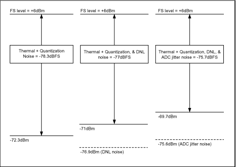
Figure 3. The MAX1428 ADC noise contributions illustrated in the first Nyquist region.
Blocker Absent Scenario for Receiver SensitivityAssume all the analog circuitry in front of the ADC has a cascaded noise figure of 3.5dB. Suppose the goal is for the ADC to degrade the overall receiver noise figure by no more than 0.2dB to meet some target sensitivity in a CDMA base station receiver. This noise figure value should provide sufficient margin to the air-interface requirements, which is also dependent on the final detector's Eb / No (bit energy to noise power spectral density ratio) requirement. If the MAX1428 Thermal + Quantization Noise Floor value from Table 1 is used, an equivalent noise figure of 25.7dB can be calculated (per procedure outlined in Figure 1) when the device is clocked at 80Msps. The ADC noise in the 1.23MHz CDMA channel bandwidth is 15.1dB lower than the noise in the first Nyquist region due to the processing gain achieved. All noise power in Figure 4 is calculated in the channel bandwidth unless otherwise specified. An overall gain of 35dB is calculated to achieve the desired typical noise figure value of 3.7dB.
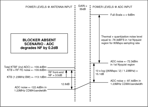
Figure 4. Blocker absent scenario.
Blocker Present ScenarioWith 35dB gain ahead of the ADC, a maximum single tone blocker level above -29dBm at the antenna terminal will exceed the ADC full-scale input. The cdma2000® cellular base station standard specifies a maximum allowable blocker level of -30dBm at the antenna terminal. In any practical application, margin to this maximum blocker level needs to be included in the design when receiver gain tolerances are taken into consideration. For this example, 6dB gain reduction is used to increase the largest allowable blocker signal applied to the ADC . This amount of gain reduction results in a maximum blocker level of -25dBm at the antenna and + 4dBm (at -2dBFS) at the ADC input. The cdma2000 air-interface standard allows 3dB degradation in overall (noise + distortion) relative to reference sensitivity when a single-tone blocker is present. The allocation of (noise + distortion) components is left up to the designer for any particular receiver configuration. As an example, su ppose the designer allows the RF front-end cascaded noise figure to degrade by 0.5dB (from the nominal 3.5dB) when 6dB of AGC is applied. With only 29dB of gain in front of the ADC and an effective noise figure of 28.3dB, the cascaded receiver noise figure is 5.3dB in the 'blocked condition', which is a 1.6dB degradation from 3.7dB noise figure calculated for receiver sensitivity. This is 1.4dB less than the 3dB degradation (noise + distortion) allowed in the cdma2000 standards .
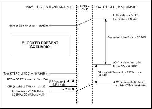
Figure 5. Blocker present scenario.
ADC Noise and Distortion (SINAD) If the ADC's SINAD value of 72.5dB were used instead of SNR (taking into account the ADC's noise and distortion components), the overall degradation in noise figure due to the RF front-end noise figure and ADC ( noise + distortion) would be 2.1dB, which is still below the allocated 3dB for this measurement. Therefore, 0.9dB degradation is still allocated for the (noise + distortion) performance of the analog front-end of the receiver if needed.
ConclusionThis application note illustrates that the ADC generates different levels of noise power depending on the signal-input level, and that the ADC noise affects the overall receiver response for small- and large-signal level extremes. If cascaded contributions of the ADC noise (and distortion) power is not properly accounted for in the receiver design, the converter might be either over or under specified for any particular application.
Notes
1. 10 × log Feq = 10 × log (F1 + (F2-1) / G1 + (F3-1) / G1G2 + ... + (Fn-1) / G1G2 ... G (n-1))
References Digital Techniques for Wideband Receivers, James Tsui, Artech House Publishers, 1995.
RF Design Guide, Systems, Circuits, and Equations, Peter Vizmuller, Artech House Publishers, 1995.
Recommended Minimum Performance Standards for cdma2000 Spread Spectrum Base Stations, 3GPP2 TSG-C4.1, Release A, March 30, 2001.
IntroductionWhen using a high-performance Nyquist analog-to-digital converter (ADC) in a sampling or sub-sampling receiver design, an RF designer needs to know the ADC's noise performance for both small- and large-signal inputs. The receiver must meet sensitivity and blocking (high-level interference) requirements under these two signal level extremes, and the ADC generates different amounts of noise for each of these levels, which can be expressed in terms of its effective noise figure. It is important for the user to understand the amount of ADC noise contribution in the receiver line-up when determining the ADC's AC requirements. For the following discussion, it is assumed that the noise is flat across the converter's Nyquist band.
Determining the Effective Noise FigureFor small analog input signals (on the order of -35dBFS), the thermal + quantization noise power dominate the ADC noise floor, which is used to approximate the ADC's effective noise figure (NF). Once the ADC's NF is known , the cascaded noise figure equation¹ can be used to determine the overall receiver noise figure at the receiver input terminal. The level of ADC noise contribution for small-signal inputs is used for signals near and just above the receiver sensitivity. Refer to Figure 1 and use the following steps to approximate the ADC effective noise figure for small-signal analog input levels:
Calculate the ADC's full-scale level (in dBm). This step is necessary because the thermal + quantization noise power is commonly given in units of dBFS and noise figure is calculated with respect to dBm. Determine the thermal + quantization noise floor level (in dBm) either from the component vendor's data sheet or by measurement (for a small- signal input level on the order of -35dBFS). Calculate the normalized noise floor level in 1Hz-bandwidth by subtracting 10 × log (fSAMPLE / 2) where fSAMPLE is given in units of Hz. Determine thermal noise power in 1Hz bandwidth;
KTB = 4.002 × 10⁻²¹ Watts (or in log form = -174dBm), where
K = Boltzmann's constant = 1.381 × 10⁻²³ W / Hz / K,
T = 290 K at room temperature
B = Normalized bandwidth of 1Hz Calculate the effective noise figure by subtracting the result from step 4 from the result calculated in step 3. In practice, once the ADC's effective noise figure is known, and the cascaded noise figure of the analog circuitry (RF & IF) is determined; the minimum power gain ahead of the ADC is selected to meet the required receiver noise figure. The amount of power gain places an upper limit on the maximum blocker, or highest interference level the receiver can tolerate. For cellular basestation applications , the ADC often does not have sufficient dynamic range to meet both the noise figure requirements (receiver sensitivity) and maximum blocker requirements without implementing some amount of automatic gain control (AGC). The AGC can be included either in the RF or IF stages ( or both). When higher resolution converters are used, the thermal + quantization noise is lower thereby decreasing the ADC's effective noise figure. As a result, less gain is need ed in the receiver line-up to achieve the receiver noise figure thereby reducing the need for an AGC circuit when higher-level blockers are present.
Figure 1. Determining an ADC's effective noise figure for small-signal inputs for receiver sensitivity requirements.
For intermediate signal level inputs, the converter's differential non-linearity (DNL) noise increases as major subrange boundaries are traversed. The intermediate signal levels can be defined for signal levels greater than -35dBFS, but still below those input levels where clock jitter significantly increases the ADC's noise power. Intermediate signals levels are not a major focus of this application note since they are between the sensitivity and blocking signal level extremes.
For a large-level analog input signal (closer to full-scale), the ADC noise floor level increases, mainly due to clock jitter. The ratio of the signal to noise level is defined as the signal-to-noise ratio (SNR) . The acceptable level of ADC noise power in any particular application is calculated for the case when both a blocker and smaller signal are applied to the receiver terminal simultaneously. In any application, SNR can be specified for any bandwidth, however it is usually specified either in the first Nyquist region (half the sampling rate) or in the desired signal bandwidth. It is therefore very important for the user to pay close attention to the bandwidth used throughout the calculations.
Refer to Figure 2 and follow the steps below to approximate the ADC's effective noise figure for large analog input signals: Determine the converter's full-scale level (in dBm) knowing the maximum allowable VP-P and input terminating resistance, RIN. Note the level from which SNR is either specified in the manufacturer's data sheet or measured by the user (shown as X dB in Figure 2). With SNR known, calculate the converter's noise power in the first Nyquist region (in dBm). Using the sample rate, calculate 10 × log (fSAMPLE / 2) where fSAMPLE is given in units of Hz. Determine the converter's noise power in a 1Hz bandwidth by subtracting the results obtained in (4) from the results in (3). Calculate KTB for B = 1Hz (equal to -174dBm at room temperature). Calculate the effective noise figure by subtracting the results from (6) from the results obtained in (5).
Figure 2. Determining ADC effective noise figure for large-signal inputs for receiver blocker requirements.
Numeric Example using the MAX1428The MAX1428, has the following preliminary specifications (See Table 1):
Table 1. The MAX1428 Preliminary Electrical Characteristics
| Parameter | Condition | Symbol | Typ. Value | Units |
| Resolution | N | 15 | bits | |
| Analog input Range | VID | 2.56 | Vp-p | |
| Differential Input Resistance | RIN | 1000 | Ohms | |
| Analog Bandwidth, Full Power | BW1 | 260 | MHz | |
| AC SPECIFICATIONS | fSAMPLE = 80Msps | |||
| Thermal + Quantization Noise Floor | Analog Input <-35dBFS | NF | -78.3 | dBFS |
| Signal-to-Noise Ratio | Analog Input at -2dBFS, fIN = 70MHz | SNR | 73.7 | dB |
| Signal-to-Noise and Distortion Ratio | Analog Input at -2dBFS, fIN = 70MHz | SINAD | 72.5 | dB |
The MAX1428 ADC Noise ContributionsAssume that a terminating resistance placed across the differential input pins of the MAX1428 produces a total differential resistance of 200Ω. The full-scale input level is calculated to approximately equal +6 dBm (2.5VP-P across 200Ω). For a clock rate of 80Msps, the thermal + quantization noise-floor power equals -78.3dBFS or -72.3dBm in the first Nyquist region. As the 70MHz analog input level is increased above -35dBFS, but not close to full-scale, the converter DNL noise adds 1.3dB to the total converter noise floor to -71dBm. As the input level is increased further and approaches full-scale, the noise floor increases an additional 1.3dB due to ADC clock jitter to a value of -69.7dBm resulting in an effective noise figure of 28.3dB (per procedure outlined in Figure 2).
Figure 3. The MAX1428 ADC noise contributions illustrated in the first Nyquist region.
Blocker Absent Scenario for Receiver SensitivityAssume all the analog circuitry in front of the ADC has a cascaded noise figure of 3.5dB. Suppose the goal is for the ADC to degrade the overall receiver noise figure by no more than 0.2dB to meet some target sensitivity in a CDMA base station receiver. This noise figure value should provide sufficient margin to the air-interface requirements, which is also dependent on the final detector's Eb / No (bit energy to noise power spectral density ratio) requirement. If the MAX1428 Thermal + Quantization Noise Floor value from Table 1 is used, an equivalent noise figure of 25.7dB can be calculated (per procedure outlined in Figure 1) when the device is clocked at 80Msps. The ADC noise in the 1.23MHz CDMA channel bandwidth is 15.1dB lower than the noise in the first Nyquist region due to the processing gain achieved. All noise power in Figure 4 is calculated in the channel bandwidth unless otherwise specified. An overall gain of 35dB is calculated to achieve the desired typical noise figure value of 3.7dB.
Figure 4. Blocker absent scenario.
Blocker Present ScenarioWith 35dB gain ahead of the ADC, a maximum single tone blocker level above -29dBm at the antenna terminal will exceed the ADC full-scale input. The cdma2000® cellular base station standard specifies a maximum allowable blocker level of -30dBm at the antenna terminal. In any practical application, margin to this maximum blocker level needs to be included in the design when receiver gain tolerances are taken into consideration. For this example, 6dB gain reduction is used to increase the largest allowable blocker signal applied to the ADC . This amount of gain reduction results in a maximum blocker level of -25dBm at the antenna and + 4dBm (at -2dBFS) at the ADC input. The cdma2000 air-interface standard allows 3dB degradation in overall (noise + distortion) relative to reference sensitivity when a single-tone blocker is present. The allocation of (noise + distortion) components is left up to the designer for any particular receiver configuration. As an example, su ppose the designer allows the RF front-end cascaded noise figure to degrade by 0.5dB (from the nominal 3.5dB) when 6dB of AGC is applied. With only 29dB of gain in front of the ADC and an effective noise figure of 28.3dB, the cascaded receiver noise figure is 5.3dB in the 'blocked condition', which is a 1.6dB degradation from 3.7dB noise figure calculated for receiver sensitivity. This is 1.4dB less than the 3dB degradation (noise + distortion) allowed in the cdma2000 standards .
Figure 5. Blocker present scenario.
ADC Noise and Distortion (SINAD) If the ADC's SINAD value of 72.5dB were used instead of SNR (taking into account the ADC's noise and distortion components), the overall degradation in noise figure due to the RF front-end noise figure and ADC ( noise + distortion) would be 2.1dB, which is still below the allocated 3dB for this measurement. Therefore, 0.9dB degradation is still allocated for the (noise + distortion) performance of the analog front-end of the receiver if needed.
ConclusionThis application note illustrates that the ADC generates different levels of noise power depending on the signal-input level, and that the ADC noise affects the overall receiver response for small- and large-signal level extremes. If cascaded contributions of the ADC noise (and distortion) power is not properly accounted for in the receiver design, the converter might be either over or under specified for any particular application.
Notes
1. 10 × log Feq = 10 × log (F1 + (F2-1) / G1 + (F3-1) / G1G2 + ... + (Fn-1) / G1G2 ... G (n-1))
References Digital Techniques for Wideband Receivers, James Tsui, Artech House Publishers, 1995.
RF Design Guide, Systems, Circuits, and Equations, Peter Vizmuller, Artech House Publishers, 1995.
Recommended Minimum Performance Standards for cdma2000 Spread Spectrum Base Stations, 3GPP2 TSG-C4.1, Release A, March 30, 2001.
cdma2000 is a registered trademark of Telecommunications Industry Association.
48V Brushless Dc Motor,24V Brushless Dc Motor,48V Brushless Motor,80 Series Bldc Motor
Jinan Keya Electron Science And Technology Co., Ltd. , https://www.keyaservo.com