
The MAX5195 is a 14-bit, 260Msps high-speed digital-to-analog converter (DAC). Its data interface is compaTIble with high-speed low-voltage positive emitter-coupled logic (LVPECL) signals. Matched-transmission-line capabilities enable the interface to handle very high speed data signals, and its differential digital-signal inputs minimize the effects of noise originating from a printed circuit board (PCB).
High-speed FPGAs such as the Xilinx Virtex series and Altera Apex series have LVPECL-compatible outputs suitable for driving the MAX5195. The following discussion should help you achieve optimum operation while interfacing these high-speed logic devices to the MAX5195.
Xilinx Virtex InterfaceThe LVPECL outputs of Xilinx's Virtex family of FPGAs require an external resistor network to transform their output voltage and impedance levels into LVPECL-compliant signals. Such output-termination networks yield logic levels (low and high) whose DC offset differs approximately -300mV from those of true LVPECL levels. Unfortunately for the DAC, such signals exceed the low-voltage limit for its LVPECL inputs.
To adapt their quasi-LVPECL outputs to true LVPECL output levels, Xilinx suggests a simple modification to the network (Figure 1): add two resistors for each differential connection. The suggested network is shown below, coupling a single differential pair of output signals from a Virtex FPGA to the MAX5195. The resistors help to offset the output voltages by + 300mV, thereby centering those voltages about the true LVPECL levels. The resistors also eliminate violations of input range on the MAX5195's low-voltage side.
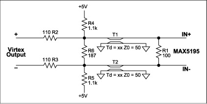
Figure 1. Xilinx's Virtex family resistor network to drive the MAX5195.
Resistors R2-R6 should be placed at the Virtex FPGA source pins, forming a 100Ω differential source impedance. Two 50Ω transmission lines connect this source to the remote MAX5195 input pins, and R1 connects across the MAX5195 LVPECL inputs to provide a 100Ω differential load impedance . Using the following resistor values, you can replicate that network for each of the 14 LVPECL data pairs.
| Resistor Values | |
| R1 | 100Ω |
| R2, R3 | 110Ω |
| R4, R5 | 1.1kΩ |
| R6 | 187Ω |
The network yields a 100Ω matched-impedance system (source, line, and termination) that maintains excellent logic-signal fidelity. Because Virtex drivers exhibit fast transition times, the trace lengths interconnecting the resistor networks should be less than 1cm long (0.39 inches) . Logic levels at the receiver inputs are VOH = 2.32V and VOL = 1.62V, which places them in the middle of the LVPECL input range.
Altera Apex InterfaceAs shown in Figure 2, LVPECL outputs of the Altera Apex series of FPGAs also require an external resistor network to transform impedance and voltage levels into LVPECL-compliant signals. Again, the network couples one differential pair of output signals from an Apex FPGA to the MAX5195.
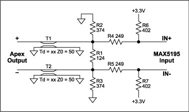
Figure 2. Apex Family resistor network to drive the MAX5195.
Resistors R1-R7 should be placed at the MAX5195 input pins. The network then forms a 100Ω termination resistance for two 50Ω transmission lines from the FPGA outputs. Again, fast transition times at the Apex driver outputs require that trace lengths interconnecting the resistor network and MAX5195 inputs should be less than 1cm long (0.39 inches).
| Resistor Values | |
| R1 | 124Ω |
| R2, R3 | 374Ω |
| R4, R5 | 249Ω |
| R6 | 402Ω |
Logic levels at the receiver inputs are VOH = 2.33 V and VOL = 1.55 V, which places them within the LVPECL input range.
SummaryThe MAX5195 DAC includes a high-speed, low-noise, differential LVPECL interface. Modern high-speed FPGAs are capable of driving the MAX5195 very effectively, but they typically require a matching resistor network to optimally drive LVPECL loads. With an appropriate network, the interface delivers speed and low-noise capability as well.
Headphone speaker is a king of speaker unit which is used for headphone, it also called headphone driver. These speakers have high sound pressure level, fast frequency response, wide frequency response range and low distortion. Headphone Speakers are mainly used for voice headphone (e.g. customer service phone, call center headphone, military intercom headset- ) and music headphone (e.g. Bluetooth headphone, sport headphone, game headphone-).
Our main headphone speakers include:
1) From the diameter, we have speakers in 23mm ~ 57mm.
2) From the impedance, we have speakers of 32ohm/150ohm/300ohm/1000ohm.


FAQ
Q1. What is the MOQ?
XDEC: 2000pcs for one model.
Q2. What is the delivery lead time?
XDEC: 15 days for normal orders, 10 days for urgent orders.
Q3. What are the payment methods?
XDEC: T/T, PayPal, Western Union, Money Gram.
Q4. Can you offer samples for testing?
XDEC: Yes, we offer free samples.
Q5. How soon can you send samples?
XDEC: We can send samples in 3-5 days.
Intercom Headphone Speaker,Call Center Headphone Speaker,Military Headphone Speaker,Voice Headphone Speakers
Shenzhen Xuanda Electronics Co., Ltd. , https://www.xdecspeaker.com