
Design of GP-IB interface circuit based on PCI bus
Abstract: It mainly introduces how to design a PCI bus interface circuit according to the PCI bus protocol as a slave device, so as to realize the design of the GP-IB interface circuit based on the PCI bus.
Foreword
The block diagram of the GP-IB interface circuit based on the PCI bus is shown in Figure 1. The industrial control computer adopts the PCI-104 stack structure and is connected to the EPLD through the PCI bus. The data bus is 32bit and the transmission rate is 33MHz. EPLD completes the design of the PCI bus interface circuit and the control of the NAT9914 interface chip, and completes the GP-IB interface communication through the driver chips 75160 and 75162. Here we focus on the internal circuit design of EPLD.
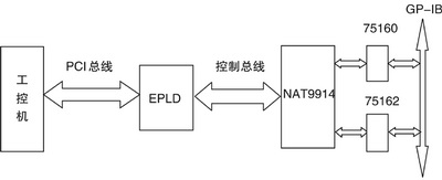
Figure 1 GP-IB interface circuit block diagram
EPLD internal circuit design
The PCI local bus is very complicated, and the PCI local bus is also constantly developing. Now bus standards such as CPCI and PCI Express have been derived. The definition of the PCI local bus is very powerful. Of course, if all the requirements of the PCI local bus can be realized, it is the best choice to purchase a dedicated integrated circuit or IP core for the PCI local bus, because the hardware design of the PCI local bus is too large. It is difficult to achieve all. If the device is only a slave device, it is not very complicated to implement according to the design requirements. Many functions such as arbitration, boundary scan, and error reporting can be eliminated, even functions such as parity, retry, and burst transmission No need to achieve.
According to the function of the GP-IB interface card, this article mainly introduces the design of the PCI bus interface circuit implemented in the EPLD, and can correctly operate the control chip NAT9914 of the GP-IB bus protocol. The capacity of EPLD is small, we use XC95288XL device of XILINX company, there are only 288 macrocells, after design optimization, and finally successfully loaded. The block diagram of its implementation is shown in Figure 2.
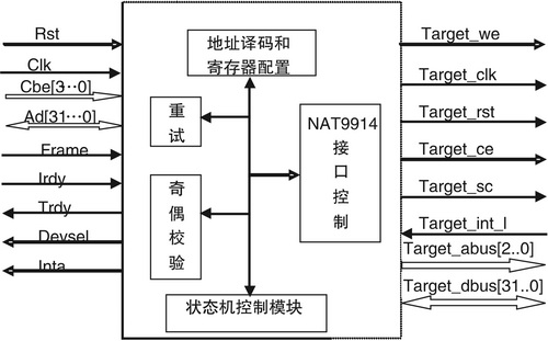
Figure 2 EPLD internal circuit block diagram
PCI interface signal design
The design of PCI interface signals is critical. There are many signals defined by the PCI bus specification, and there must be trade-offs in the design process. The following interface signals are designed according to the requirements of the PCI bus specification and the actual needs of the design circuit:
Rst: Power-on reset signal, active low.
Clk: 33MHz clock signal.
Cbe [3..0]: Command, byte enable signal.
Ad [31..0]: Three-state input / output signal multiplexed with address and data.
Frame: Frame period signal, driven by the master device, indicating the current start and duration of a transaction by the master device.
Irdy: The master device is ready for signal.
Trdy: The signal is ready from the device data.
Devsel: The slave device is selected to respond to the signal.
Inta: Slave device interrupt request, active low.
The signals discarded during design are: Par, Stop, Perr, Serr, Req, Gnt.
GP-IB interface chip control signal design
According to the circuit requirements, the following interface signals are designed to complete the control of NAT9914 and driver chip, and realize the conversion of PCI to GP-IB interface.
Target_clk: GP-IB interface control chip clock, this solution is designed to divide the frequency of 33MHz clock by 8.
Target_rst: reset pulse signal, low level reset.
Target_ce: read and write enable, high level is read, low level is write.
Target_sc: Identifies the GP-IB interface card as a controller or as a normal device.
Target_we: write enable control, active low.
Target_int_l: Control chip interrupt output, active low.
Target_abus: effective address output.
Target_dbus: Three-state data input / output bus.
Circuit optimization design
Figure 2 shows the functional block diagram of the PCI bus interface circuit. Due to the small capacity of EPLD, unnecessary circuit design must be minimized and the circuit design must be optimized during the design.
Decoding circuit
There are 12 kinds of PCI bus command coding methods. In this design, we only implement four types of coding transaction: configuration read, configuration write, memory read and memory write. The decoding function circuit works in the address cycle and includes three functions: command decoding, address decoding and command / address latch. In the first clock cycle when Frame goes low, the decoding circuit decodes the command Cbe [3..0] from the master device and issues a configuration read or write or memory read and write command to the state machine control module. Latch the address.
Configuration register
In the PCI specification, the configuration space is an address space with a capacity of 256 bytes and a specific recording structure or model. The space is divided into a header area and a device-related area. Registers not used in the configuration registers will default to zero when the CPU reads them.
Retry
The GP-IB control chip register response can fully meet the requirements of the PCI specification, no retry is required, and this part of the function is no longer implemented.
Parity check
The parity check can be shielded and opened in the BIOS. In order to reduce the complexity of the design, the parity check function is not implemented in the EPLD, and it is shielded in the BIOS.
NAT9914 interface control circuit
The NAT9914 interface control circuit mainly completes the timing control from the internal bus to the peripherals. The GP-IB bus interface uses a negative logic level design. Considering the limited capacity of EPLD, data transmission does not support DMA mode at the time of design, and only supports single-cycle CPU reading and writing. Due to the large delay when the CPU reads data, it is necessary to wait for the read delay when designing the PCI state machine.
Design and implementation of state machine
The design of the state machine is the core part of the entire design. It is mainly used to control the timing of the slave devices and the PCI bus. In this design, the completion of the configuration process and the reading and writing of the memory are all done by the state machine. Due to the limited capacity of EPLD, the read-write speed of the GP-IB interface chip is relatively slow, and the burst operation of the CPU is not supported when designing the state machine. Table 1 gives the state name, state variables and description of the state machine, and Figure 3 shows the flow chart of the state machine.
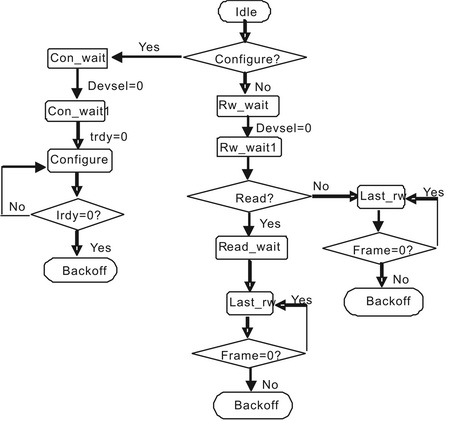
Figure 3 State machine design flow chart
The timing analysis and design points of read and write operations are given according to the flow chart of the state machine:
The PCI specification defines three read and write operations, namely Memory and I / O read and write and configuration read and write. This solution does not support I / O read and write, only supports Memory and configuration read and write, the following shows the single-cycle simulation read and write timing of Memory mapping.
Memory write operation
The timing of the single-cycle memory write operation is shown in Figure 4. When the frame is low, the read and write operation is started, and the target address ad [31..0] to be written and the command cbe [3..0] = 7 are also given. Cbe equal to 7 means write register, latch command and address from device to buffer. In the second clk, the master device turns irdy low, and at the same time gives data, the state machine runs to 6, latches the data to the buffer, and trdy and devsel change from high resistance to high level. In the third clk, devsel goes low, giving the master device a response signal, indicating that the slave device has responded to the request, and the state machine runs to 7. According to the write operation, target_we and target_ce become low, and the address is decoded and placed on the address bus, while driving the data bus, indicating that the control chip is being written. In the fourth clk, the target_ready_l of the target device is detected to be low, indicating that the slave device is ready to receive data, the state machine runs to 8, and trdy becomes low. In the fifth clk, the state machine runs to 9, trdy goes high, and at the same time the master device will drive irdy high, indicating that a write cycle is over. The state machine runs to the initial state, waiting for the next operation. target_ce and target_we will increase the delay and end the control chip write cycle.
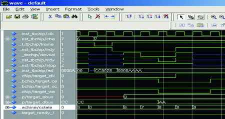
Figure 4 Timing of memory write cycle
Memory read operation
The sequence of single-cycle memory read operation is shown in Figure 5. When the frame is low, the read and write operation is started, and the target address to be written is ad [31..0] and the command cbe [3..0] = 6 The slave device latches the command and address. In the second clk, the state machine runs to 6, enters the read and write wait state, the master device changes the frame high, indicating single-cycle mode, trdy, devsel, from high resistance to high level. In the third clk, the state machine runs to 7, and gives the response signal devsel, detects that target_ready_l is high, the state machine enters the wait state until it is low, and then runs to read wait state 4. In state machine 8, trdy goes low and the slave device places the read data on the ad [31..0] bus. In the state machine 9, trdy goes high, devsel goes high, and at the same time, the master device goes irdy high, ending the single-cycle read operation. Devsel and trdy return to the high-impedance state, and the state machine runs to the initial state, preparing for the next operation.

Figure 5 Timing of memory read cycle
Conclusion
This design occupies less chip resources and is highly portable. Design changes can be made according to the different needs of the equipment, and it has been widely used in many test instruments.
references:
1. Li Guishan, Chen Jinpeng, PCI local bus and its application, Xidian University Press, 2003
2. Hou Boheng, Gu Xin, VHDL hardware description language and circuit design, Xidian University Press, 1997
- [Stellar HD Night Vision]Backup camera upgraded to Stellar HD for improved night vision. Backup cameras with stellar HD night vision no need to worry about blind spots when reversing your car
- [175° Wide Viewing Angle]This little car Rear View Camera have a wider viewing angle than other brands.Diagonal of 175 degrees, horizontal of 140 degrees and 90 degrees in the vertical direction
- [High resolution image]This HD backup camera have resolution of 1280 X 720 pixels,It can be used on the HD screen, the clearer image compared to other vehicle backup cameras
- [Universal mounted] The universal mount backup camera can be installed on all 12V cars. Different position can be achieved with the adjustable bracket.No built-in guidelines give you a clearer view
-
[32ft video cable & easy install]We offer 32ft video cable to ensure rear view camera can perfect fit for most types of cars .The installation is only 3 steps, really simple for you to install and running in few minutes.

Hd Reverse Camera,Stellar Hd Reverse Camera,Backup Camera Oem,Side View Backup Camera
Shenzhen Sunveytech Co.,LTD , https://www.sunveytech.com