
1. Introduction
The development and application of single-chip microcontrollers have become deeply integrated into various aspects of daily life. One significant application is the mass programming of chips with limited memory, where a high-speed programmer with stable performance is essential for large-scale chip burning by major manufacturers. While the 89C51-based programmers are widely used in the market, their limited functionality struggles to meet the growing demands of modern applications. This paper presents a novel programmer that uses the MSP430F149 microcontroller as its core control unit. Compared to traditional 51 MCU programmers, this design introduces an I2C memory module, allowing chip programming without the need for a computer, thus making the process more efficient and user-friendly.
2. System Design
The programmer based on the MSP430F149 consists of several key modules: a keyboard, display, serial communication interface, programming interface, level shifting circuit, power supply, and storage module. The system architecture is illustrated in Figure 1, showing the integration of all components to support the programming functions effectively.
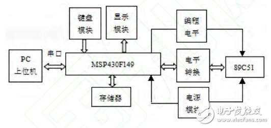
Figure 1: System Block Diagram
3. Hardware Circuit Design of the Programmer
3.1 CPU Module
The core of the programmer is the ultra-low-power MSP430F149 microcontroller. As shown in Figure 2, the minimum system includes crystal oscillators Y1 and Y2, a reset circuit, data transmission ports P1, address lines P3.0–P3.4 and P4, and connections to the keyboard (P5.3, P5.4), LCD (P2, P5.0–P5.2), and memory (P3.6, P3.7).
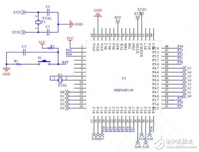
Figure 2: MSP430F149 Minimum System Schematic
3.2 Serial Port Module
To ensure compatibility between the MSP430F149 and the host computer, the MAX232 chip is used for signal level conversion. It operates on a single +5V power supply and supports RS-232 communication standards, enabling reliable data exchange between the programmer and the computer.
3.3 Storage Module
The storage module features an I2C-based EEPROM, specifically the AT24C16 chip, which provides 8 KB of memory. As shown in Figure 3, the SDA and SCL lines connect the MSP430F149 to the AT24C16, allowing the programmer to store program data for offline operations.
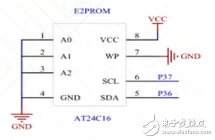
Figure 3: Storage Module Connection Diagram
3.4 Keyboard and Display Module
The keyboard module utilizes a PS2 interface, known for its reliability and simplicity, using only two signal lines. It is primarily used for function selection during programming. The display module employs a 1602 LCD to show chip type, voltage, and operation status, as illustrated in Figure 4 and 5.
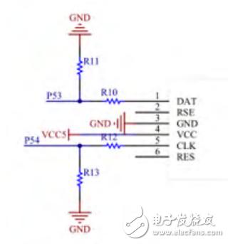
Figure 4: Keyboard Module Circuit Schematic
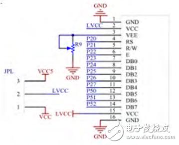
Figure 5: Display Module Circuit Schematic
3.5 Power Module
The power module supplies 3.3V to the MSP430F149 and 12V to the 89C51 chip. A voltage regulator (ASM1117-3.3V) converts the +5V input to 3.3V, while the 51 chip directly receives +5V and generates the required 12V for programming, as shown in Figure 6.

Figure 6: Power Module Connection Diagram
3.6 Programming Module
The programming module interfaces with the 89C51 chip, utilizing P0.0–P0.7 for data input, P1.0–P1.7 for low address, and P2.0–P2.3 for high address. As shown in Figure 7, 74LVC8T245 buffers handle voltage level conversion between 3.3V and 5V, ensuring compatibility and signal integrity.
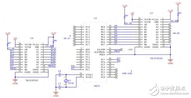
Figure 7: 89C51 Programming Connection Diagram
4. Programmer Functions and Software Design
The programmer supports read, write, verify, and erase functions. These can be executed either through command mode when connected to a computer or via keyboard input in standalone mode. Communication between the upper and lower systems ensures seamless data transfer.
As shown in Figure 8, the programmer enters an interrupt state upon receiving data. It checks if the data is a command (e.g., "Check", "Erase", "Read", "Write") and executes the corresponding action. If it’s not a command, it treats it as data and stores it in the EEPROM.
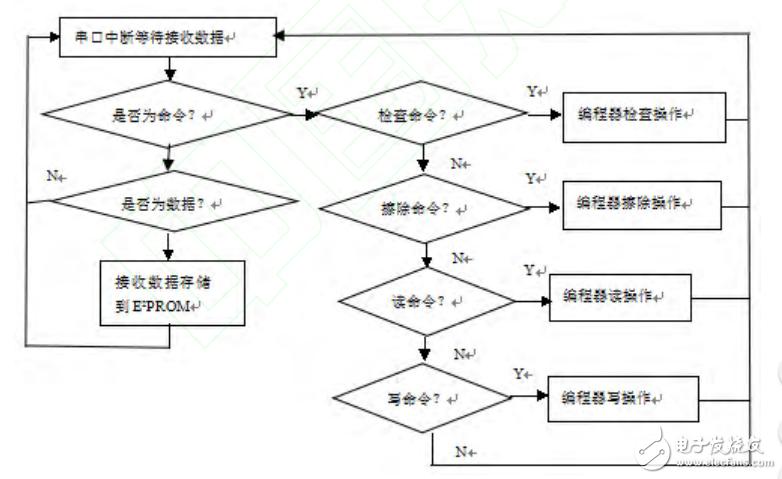
Figure 8: Serial Communication and Online Programming Flow
As shown in Figure 9, the offline software flow allows users to input commands like "Check#", "Erase#", "Read#", "Write#", "Verify#", or "Auto#". Each command triggers specific actions, such as checking flash memory, erasing, reading, writing, verifying, or performing a full sequence of operations, with results displayed on the LCD.
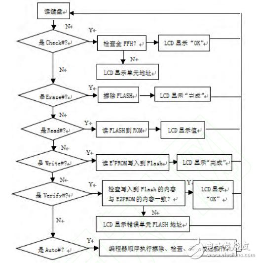
Figure 9: Offline Programming Software Flow
The main functions of the programmer are implemented in C code, including initialization, read, write, erase, check, and verification functions. The main loop handles user input and controls the overall operation of the system.
5. Conclusion
This paper presents a programmer based on the MSP430F149 microcontroller, designed to perform programming tasks on 89C51 series chips efficiently. Through practical testing, the programmer has demonstrated fast and independent operation, significantly improving the speed and stability of chip programming. Its enhanced functionality and user-friendly design make it a valuable tool in industrial and educational settings.
The primary purpose of any fuse cutouts is to provide protection to the lines of your system and the various apparatus on those lines such as transformers and capacitor banks. Fuse cutouts provide reliable protection from low-level overloads that just melt the fuse link, intermediate faults, and very high faults, through maximum interrupting capacity.
Fuse Cutout,Fuse Cutout Amperes,Porcelain Fuse,Cut Out Fuse Carrier
Jilin Nengxing Electrical Equipment Co. Ltd. , https://www.nengxingelectric.com