
Since its introduction in 1984, the capacity of field-programmable gate arrays (FPGAs) has grown by more than 10,000 times, while their performance has improved by a factor of 100. The cost and power consumption per unit function have dropped by over 1,000 times. These improvements are largely due to advancements in semiconductor process technology, but the evolution of FPGAs is far more complex than just scaling. Moore’s Law has not only driven quantitative growth but also led to significant qualitative changes in FPGA architecture, application domains, and design methodologies. As a result, FPGAs have gone through several distinct development phases. This paper outlines three key stages—Invention, Expansion and Accumulation—and explores the driving forces behind each phase along with their defining characteristics. It concludes with a glimpse into the future of FPGA technology.
Xilinx introduced the first FPGA in 1984, though it wasn’t officially called an FPGA until Actel gained popularity in 1988. Over the next 30 years, FPGA devices evolved dramatically. Their capacity increased by more than 10,000 times, speed improved by 100 times, and the cost and energy consumption per logical function dropped by over 1,000 times (see Figure 1).
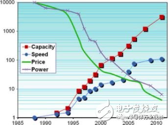
Figure 1 shows the progression of Xilinx FPGA capabilities since 1988. Capacity refers to the number of logic cells, speed represents the performance of the programmable fabric, price is measured per logic unit, and energy consumption is also per logic unit. The price and energy values are scaled up by 10,000 times for clarity. The data comes from Xilinx publications.
While much of this progress stems from process technology advancements, viewing FPGA development as a simple expansion of capacity oversimplifies the story. In reality, the journey of FPGAs has been marked by innovation, adaptation, and strategic shifts in both hardware and software.
FPGA development has passed through several distinct phases, each shaped by technological opportunities and market demands. These factors have influenced not only the physical characteristics of the devices but also the tools and methodologies used in their design. This article reviews the three major phases of FPGA evolution, each spanning approximately eight years and clearly defined in the timeline.
The three stages are:
1. **Invention Stage (1984–1991)**
2. **Expansion Phase (1992–1999)**
3. **Accumulation Stage (2000–2007)**
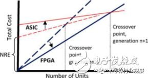
Figure 2 illustrates the intersection point between FPGA and ASIC technologies. It shows how the total cost and quantity of units influence the choice between these two approaches. The FPGA line starts lower on the left, reflecting lower initial costs but higher per-unit prices. As process nodes advance, the intersection moves, indicating that for larger volumes, ASICs become more cost-effective.
**Second, the Foreword: Key Issues in FPGA**
**A. FPGA vs. ASIC**
In the 1980s, ASICs became a popular solution in the electronics industry, offering custom integrated circuits tailored to specific applications. By the mid-1980s, many companies were selling ASICs, and competition drove the demand for low-cost, high-capacity, and fast solutions. When FPGAs emerged, they weren’t superior in all aspects, but they offered a unique advantage.
ASICs rely on custom mask tools, which require one-time engineering (NRE) costs. These costs can be very high, making ASICs less attractive for small production runs. FPGAs, on the other hand, eliminate this upfront cost by allowing multiple users to share the same silicon design. This enables FPGA vendors to spread out NRE expenses across many customers, reducing per-unit costs for end users.
The early NRE costs made FPGAs more cost-effective than ASICs for certain quantities. Vendors often highlight this in their “intersection†charts, showing where the total cost of an FPGA becomes more expensive than an ASIC. In Figure 2, the graph compares the total cost of a unit based on quantity. While ASICs have high initial NRE costs, their per-unit cost decreases after the first batch. FPGAs, without NRE charges, have a steeper slope, but their per-unit cost is higher. The two lines meet at the intersection point, where the cost of using an FPGA becomes more expensive than an ASIC.
Over time, as process technology advances, the NRE cost for ASICs increases, but the per-chip cost decreases. This pushes the intersection point higher, meaning fewer customers will find ASICs economically viable. Custom chips remain optimal for high-performance or high-volume applications, while most others benefit from the flexibility of programmable solutions.
The 433MHz, 868MHz, and 915MHz antennas are essential components in wireless communication systems, particularly in the realm of low-power wide-area networks (LPWANs), Internet of Things (IoT) applications, remote monitoring systems, and wireless data transmission. These frequency bands offer unique advantages for various communication needs, making them popular choices among device manufacturers and network operators. Each of these antennas, tailored to their respective frequency bands, ensures reliable and efficient signal transmission over long distances, facilitating seamless connectivity in diverse environments.
Frequency Bands and Their Uses
433MHz: This frequency band is often used for short-to-medium range communication due to its good propagation characteristics in the environment. It's suitable for applications that require low data rates but reliable connectivity over relatively long distances, such as remote sensor networks and asset tracking.
868MHz: The 868MHz band is widely adopted in Europe for IoT and LPWAN technologies like LoRaWAN. It offers a good balance between transmission range and data throughput, making it ideal for smart city applications, agricultural monitoring, and industrial IoT solutions.
915MHz: Operating in the 915MHz band, antennas are commonly used in North America for similar IoT and LPWAN applications as 868MHz. This frequency range provides similar performance characteristics, allowing for efficient long-range communication with low power consumption.
Antenna Types and Characteristics
Antennas designed for these frequency bands can vary in type and construction, but they share several common characteristics:
Design: They can be implemented as dipole, monopole, helical, ceramic chip, or microstrip antennas, among others. The choice of antenna type depends on the specific application requirements, such as size, weight, gain, and directionality.
Gain: The gain of the antenna determines how efficiently it directs and concentrates the radio waves in a particular direction. Higher gain antennas can achieve longer transmission distances but may require more precise alignment.
Polarization: Typically, these antennas are vertically polarized, meaning the electric field vectors oscillate in a vertical plane. This is suitable for most terrestrial communication scenarios.
Material: The antenna elements are often made of conductive materials like copper or aluminum, while the housing or support structure may be made of plastic, fiberglass, or other non-conductive materials for durability and weather resistance.
433MHz Antenna,868MHz Antenna,915MHz Antenna,433/868/915MHz Antenna
Yetnorson Antenna Co., Ltd. , https://www.yetnorson.com