
1. Introduction
The integration of single-chip microcontrollers into daily life has become widespread, especially in the field of mass chip programming. One of the key applications is the use of high-speed programmers with stable performance to meet the demands of large-scale chip burning by major manufacturers. While the 89C51-based programmer remains popular due to its simplicity, it lacks the versatility needed for modern applications. This paper presents a new programmer design that uses the MSP430F149 microcontroller as the central control unit. Compared to traditional 51 MCU programmers, this system introduces an I2C memory module, enabling standalone chip programming without the need for a computer. This feature enhances convenience and speeds up the overall process.
2. System Design
The programmer based on the MSP430F149 consists of several key modules: a keyboard, display, serial communication interface, programming interface, level shifting circuit, power supply, and an I2C storage module. The block diagram of the system is shown in Figure 1, illustrating how these components interact to support efficient and reliable chip programming.
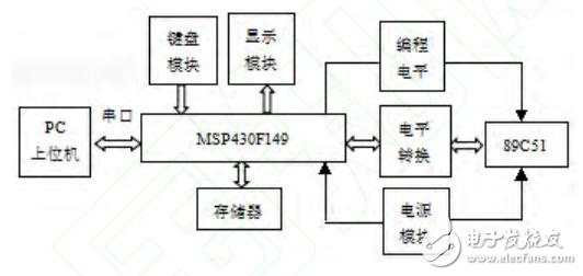
Figure 1: System Block Diagram
3. Hardware Circuit Design
3.1 CPU Module
The core of the programmer is the ultra-low-power MSP430F149 microcontroller. The minimum system schematic is shown in Figure 2, which includes the crystal oscillators (Y1, Y2), reset circuit (RST), data port (P1), address lines (P3.0–P3.4 and P4), keyboard interface (P5.3, P5.4), LCD connections (P2, P5.0–P5.2), and memory interface (P3.6, P3.7).
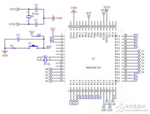
Figure 2: MSP430F149 Minimum System Schematic
3.2 Serial Port Module
To ensure compatibility between the MSP430F149 and the host computer, the MAX232 chip is used for signal level conversion. This RS-232 compatible interface allows seamless communication between the programmer and the host system using a single +5V power supply.
3.3 Storage Module
The I2C memory module uses the AT24C16 EEPROM with 8 KB of storage capacity. As shown in Figure 3, the SDA and SCL lines connect the MSP430F149 to the memory, allowing program data to be stored for offline programming tasks.
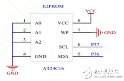
Figure 3: I2C Memory Module Connection Diagram
3.4 Keyboard and Display Module
A PS2 keyboard is used for user input, offering a simple and reliable interface with only two signal lines. The 1602 LCD displays important information such as chip type, voltage, and operation status. The connection diagram is shown in Figures 4 and 5.
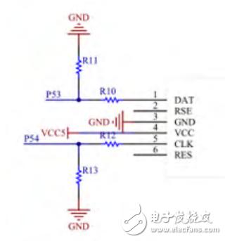
Figure 4: Keyboard Module Circuit Schematic
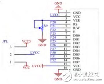
Figure 5: LCD Module Circuit Schematic
3.5 Power Module
The power module provides 3.3V for the MSP430F149 and 12V for the 89C51 chip. A voltage regulator (ASM1117-3.3V) converts +5V to 3.3V, while the 51 chip is powered directly from the same source to generate the required programming voltage.
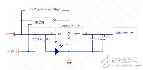
Figure 6: Power Module Connection Diagram
3.6 Programming Module
The programming module interfaces with the 89C51 chip through the 74LVC8T245 level shifter, which handles voltage conversion between 3.3V and 5V. The address and control signals are managed via the DIR pin, which determines the direction of data flow.
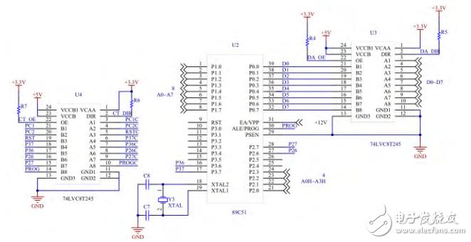
Figure 7: 89C51 Programming Connection Diagram
4. Programmer Function and Software Design
The programmer supports read, write, verify, and erase functions. These operations can be performed either through command mode when connected to a computer or via keyboard input when operating offline. Communication between the upper and lower systems is handled through serial ports.
As illustrated in Figure 8, the system enters an interrupt state to receive commands. If a command is received, it is processed accordingly—either as a read, write, erase, or verification request. Otherwise, the system continues to wait for incoming data.
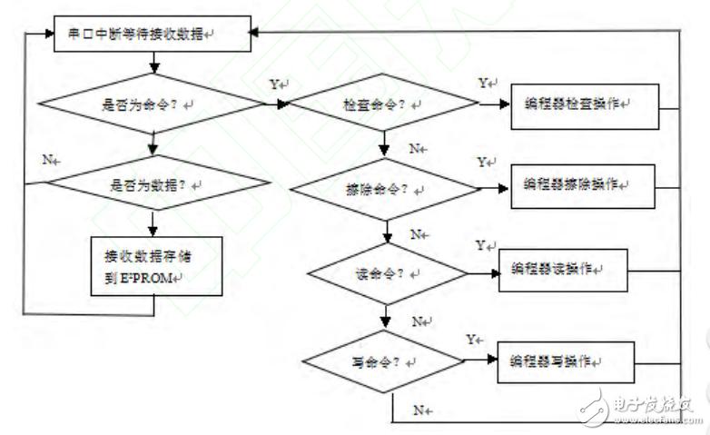
Figure 8: Flow Chart of Serial Communication and Online Programming
Figure 9 shows the offline programming flow, where the user inputs commands like "Check#", "Erase#", "Read#", "Write#", "Verify#", or "Auto#". The system performs the corresponding action and displays results on the LCD.
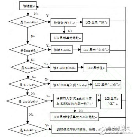
Figure 9: Offline Programming Software Flow Chart
The main functions of the programmer are implemented through various subroutines, including initialization, reading, writing, erasing, checking, and verifying data. The code structure is as follows:
5. Conclusion
This paper demonstrates a practical solution for programming 89C51 chips using the MSP430F149 microcontroller. The designed programmer offers faster and more efficient chip programming capabilities, with improved stability and ease of use. It is particularly suitable for scenarios requiring independent, offline operation, making it a valuable tool for industrial and educational applications.
The Zinc Oxide Type Surge Arrester is the latest advanced over-voltage protector for distribution line and power stationdevice. Incorporated with zinc oxide and other metal oxide as the core resistor disc, the volt-ampere characteristics and thethrough-current capability of the resistor disc are improved drastically compared with the conventional SiC type surge arrester.
Under nominal operating voltage, the current through the surge arrester is only about micro-ampere grade. When the surgearrester experiences an over-voltage, the resistor disc with excellent non-inear characteristics will increase the curent throughthe surge arrester to several thousand amperes instantaneously, The surge arrester is in a conducting state and then will releasethe over-voltage energy to the earth and thereby protects power distribution / transmission device against the impact of over voltage.
Ceramic Arrester,Ceramic Lightning Arrester,Housing Surge Arrester,Lightning Arrester Antenna
Jilin Nengxing Electrical Equipment Co. Ltd. , https://www.nengxingelectric.com