
The switching tube is turned on and off theoretically in an instant, but in reality, there is an overlap time between the falling current and the rising voltage at the time when the switching tube is turned off, so there is a large turn-off loss. In order to effectively suppress the IGBT turn-off process voltage and reduce the turn-off loss, it is usually necessary to provide a turn-off snubber circuit for the IGBT main circuit. In general, when designing the snubber circuit for IGBT, it is necessary to comprehensively consider the main circuit structure and device capacity from the IGBT application, and the IGBT turn-on characteristics and turn-off characteristics required to meet various technical specifications of the main circuit.
The RCD snubber circuit is selected, and the structure is shown in Figure 4-5.
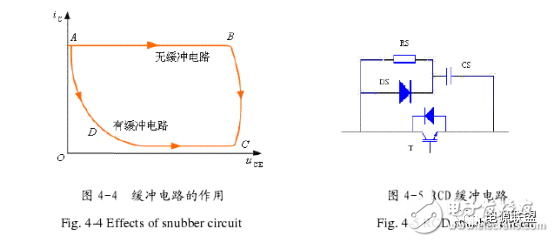
Requirements for the snubber circuit: Minimize the inductance of the main circuit; the capacitor should use low-sensitivity absorbing capacitor; the diode should use fast turn-on and fast recovery diode to avoid large oscillating overvoltage caused by open-pass voltage and reverse recovery.

3) Selection of snubber diode
The fast recovery diode ERA34-10 is used with a parameter of 0.1A/1000V/0.15us.
What is the role of the relay RC plus absorption unit?
When the contactor and relay are powered off, a surge pulse is generated when the coil is released. This surge voltage may interfere with some sensitive electronic devices, causing the electronic device to malfunction or malfunction. Therefore, the contactor and the relay coil are connected in parallel. A RC absorber absorbs this pulse.
Generally, the contactor or relay of the absorption unit is installed because there are sensitive electronic circuits in the same circuit. These circuits are sensitive to surge pulses, so the contactor or relay in this type of circuit is equipped with an absorption unit and an absorption relay. The pulse and surge generated by the coil release, to avoid malfunction or malfunction of the electronic circuit.
The role of the RC absorption loop is to clamp the self-induced electromotive force of the inductive device during current transients, and to suppress the impact of the device on the device due to dV/dt. In the inductive load, the switching device is turned off. At the moment, if the magnetic flux of the inductive load is not zero at this time, according to Lenz's law, a self-induced electromotive force will be generated, and the external magnetic field will be stored for the sake of simplicity. For the sake of simplicity, the RC absorption loop is generally used. Energy is dissipated as thermal energy.
To design the RC absorption loop parameters, you need to determine the size of the magnetic field energy storage. There are several cases:
1. The motor, relay, etc., its excitation inductance is connected in series with the main circuit. The magnetic field energy storage needs to be completely processed by the RC circuit. When the switching device is turned off, the initial current of the RC circuit is equal to the working current before the shutdown;
2. Power frequency transformer and forward transformer, its excitation inductance is parallel with the main circuit, and the excitation current is much smaller than the working current. Although the magnetic field energy storage needs to be completely processed by the RC loop, the initial current of the RC loop is much smaller than the operating current before the shutdown, at the moment when the switching device is turned off.
3. The flyback transformer, the magnetic field energy storage is resigned by two parts, most of which provide energy to the secondary side through mutual inductance, and only the leakage inductance part is processed by the RC loop.
In the above three cases, it is necessary to measure the magnetizing inductance, mutual inductance and leakage inductance value, and then obtain the initial current value of the RC loop.
The value of R is the instantaneous back pressure that the switch can withstand, compared with the initial current value; if the value is too small, the dynamic power consumption is too large, and if the value is too large, the protection switch is not achieved;
RC absorption loop design basis
The role of the RC absorption loop is to clamp the self-induced electromotive force of the inductive device during current transients, and to suppress the impact of the device on the device due to dV/dt . In the inductive load, the switching device is turned off. At the moment, if the magnetic flux of the inductive load is not zero at this time, according to Lenz's law, a self-induced electromotive force will be generated, and the external magnetic field will be stored for the sake of simplicity. For the sake of simplicity, the RC absorption loop is generally used . Energy is dissipated as thermal energy.
To design the RC absorption loop parameters, you need to determine the size of the magnetic field energy storage. There are several cases:
1. Motor, relay, etc., its excitation inductance is connected in series with the main circuit. The magnetic field energy storage needs to be completely processed by the RC circuit. When the switching device is turned off, the initial current of the RC circuit is equal to the working current before the shutdown; 2. Power frequency Transformer, forward transformer, its magnetizing inductance is connected in parallel with the main circuit, and the excitation current is much smaller than the working current. Although the magnetic field energy storage needs to be completely processed by the RC loop, the initial current of the RC loop is much smaller than the operating current before the shutdown, at the moment when the switching device is turned off . 3 , flyback transformer, magnetic field energy storage by two parts of the resignation, most of them through the mutual inductance to the secondary side to provide energy, only the leakage inductance part to be processed through the RC loop,
In the above three cases, it is necessary to measure the magnetizing inductance, mutual inductance and leakage inductance value, and then obtain the initial current value of the RC loop.
The value of R is the instantaneous back pressure that the switch can withstand, compared with the initial current value; if the value is too small, the dynamic power consumption is too large, and if the value is too large, the protection switch cannot be achieved;
The value of C needs to satisfy half of the magnetic energy that can be stored at the clamp level, and meets a certain dV/dt.
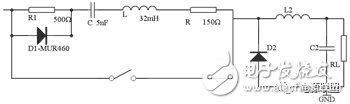
Electromagnetic compatibility design of switching power supply (EMC design ) - snubber circuit for reducing interference source interference energy
A snubber circuit (as shown) is added to the input of the switch control power supply, which consists of a linear impedance stabilizing network to eliminate potential interference such as power line disturbances, electrical fast transients, surges, voltage levels, and power line harmonics. Device parameters for the buffer circuit D1 is MUR460, R1 = 500Ω, C = 6nF, L = 36mH, R = 150Ω.
RCD absorption circuit design
For a switching power supply engineer, it is common to make choices in the face of one or more opposing conditions. And the topic we are discussing today is a pair of opposing conditions. (ie, to limit the maximum reverse peak of the main MOS tube, and to minimize the power consumption of the RCD absorption loop) Let us make a few assumptions before discussion. 1    Switching power supply operating frequency range: 20 ~ 200KHZ; the diode forward in time ② RCD short (typically a few tens of nanoseconds); ③    After adjusting the main transformer and MOS tube before the RCD loop , the parameters of the output line have been completely determined. With the above assumptions, we can first calculate: First, segment the VD of the MOS tube : i , the input DC voltage VDC ; ii , the secondary reflection VOR ; iii , the main MOS tube VD margin VDS ; iv , RCD absorbs the effective voltage VRCD1 . Second, calculate the parts of the above main MOS tube VD : i , the input DC voltage VDC . When calculating VDC , it is based on the highest input voltage value. For wide voltage , AC265V should be selected , that is, DC375V . VDC = VAC *√2 ii , the secondary reflex primary VOR . VOR is calculated based on the maximum output voltage of the secondary output and the maximum voltage drop of the rectifier diode. For example, the output voltage is: 5.0V±5% ( calculated according to Vo = 5.25V ), and the diode VF is 0.525V (this value is at 1N5822) . Find the VF value under the rated current in the data ). VOR = (VF + Vo) * Np / Ns iii , the margin of the main MOS tube VD VDS . VDS is based on 10% of the MOS tube VD . If the VD=650 of KA05H0165R should be DC65V . VDC = VD* 10% iv , RCD absorbs VRCD . The VD of the MOS tube minus the i , iii three items left the maximum value of the VRCD . The actual selected VRCD should be 90% of the maximum value (this is mainly due to factors such as the dispersion of the various components of the switching power supply, temperature drift and time drift). VRCD = (VD-VDC -VDS)*90% Note: 1 VRCD calculates the theoretical value and then adjusts it by experiment so that the actual value agrees with the theoretical value. ② VRCD must be greater than 1.3 times the VOR. (If less than 1.3 times, the main value selection MOS transistor VD is too low) ③ VD MOS tube should be less than twice the VDC. (If more than two times, the value of the main pipe on the MOS VD too big) ④ If VRCD measured value less than 1.2 times the VOR, the RCD snubber circuit to affect the power efficiency. ⑤ VRCD ⅴ is composed of a VRCD1 and VOR, RC time constant τ determined. τ is determined by the operating frequency of the switching power supply. Generally, 10 to 20 switching power supply cycles are selected. Third, test adjustment VRCD value First assume an RC parameter, R = 100K / RJ15, C = 10nF / 1KV . Re-listing electricity should follow the principle of low pressure and high pressure first, then light load to heavy load. The voltage value on the RC component should be closely monitored during the test , making sure that the VRCD is less than the calculated value. If it is found that the calculated value is reached, it should be powered off immediately. After the R value is reduced, repeat the above test. ( The voltage value on the RC component is observed with an oscilloscope. The ground of the oscilloscope is connected to the RC point of the “ + †pole of the input electrolytic capacitor , and the test point is connected to another point of the RC .) A suitable RC value should be at the highest input voltage. Under the heaviest power load, the experimental value of VRCD is equal to the theoretical calculation. Fourth, the phenomenon worth noting in the test The lower the input grid voltage, the higher the VRCD , the higher the load, the higher the VRCD . Then, at the lowest input voltage and heavy load, if the test value of VRCD is greater than the theoretically calculated VRCD value, is it contradictory to the content of (3)? Not at all contradictory, the theoretical value is the result of the calculation at the highest input voltage, but now it is the low input voltage. Heavy load is the maximum load that the switching power supply can reach. Mainly through the test to measure the ultimate power of the switching power supply. 5. The power selection of the R value in the RCD absorption circuit The power selection of R is calculated based on the maximum value of the measured VRCD . The actual selected power should be greater than twice the calculated power. Editor's Note: If the R value in the RCD absorption circuit is too small, the efficiency of the switching power supply will be reduced. However, if the R value is too large, the MOS tube is in danger of being broken down.
RCD absorption circuit design
Let's make a few assumptions before the discussion, 1    Switching power supply operating frequency range: 20 ~ 200KHZ; the diode forward in time ② RCD short (typically a few tens of nanoseconds); ③    After adjusting the main transformer and MOS tube before the RCD loop , the parameters of the output line have been completely determined. With the above assumptions, we can first calculate: First, segment the VD of the MOS tube : i , the input DC voltage VDC ; ii , the secondary reflection VOR ; iii , the main MOS tube VD margin VDS ; iv , RCD absorbs the effective voltage VRCD1 . Second, calculate the parts of the above main MOS tube VD : i , the input DC voltage VDC . When calculating VDC , it is based on the highest input voltage value. For wide voltage , AC265V should be selected , that is, DC375V . VDC = VAC *√2 ii , the secondary reflex primary VOR . VOR is calculated based on the maximum output voltage of the secondary output and the maximum voltage drop of the rectifier diode. For example, the output voltage is: 5.0V±5% ( calculated according to Vo = 5.25V ), and the diode VF is 0.525V (this value is at 1N5822) . Find the VF value under the rated current in the data ). VOR = (VF + Vo) * Np / Ns iii , the margin of the main MOS tube VD VDS . VDS is based on 10% of the MOS tube VD . If the VD=650 of KA05H0165R should be DC65V . VDC = VD* 10% iv , RCD absorbs VRCD . The VD of the MOS tube minus the i , iii three items left the maximum value of the VRCD . The actual selected VRCD should be 90% of the maximum value (this is mainly due to factors such as the dispersion of the various components of the switching power supply, temperature drift and time drift). VRCD = (VD-VDC -VDS)*90% Note: 1 VRCD calculates the theoretical value and then adjusts it by experiment so that the actual value agrees with the theoretical value. ② VRCD must be greater than 1.3 times the VOR. (If less than 1.3 times, the main value selection MOS transistor VD is too low) ③ VD MOS tube should be less than twice the VDC. (If more than two times, the value of the main pipe on the MOS VD too big) ④ If VRCD measured value less than 1.2 times the VOR, the RCD snubber circuit to affect the power efficiency. ⑤ VRCD ⅴ is composed of a VRCD1 and VOR, RC time constant τ determined. τ is determined by the operating frequency of the switching power supply. Generally, 10 to 20 switching power supply cycles are selected. Third, test adjustment VRCD value First assume an RC parameter, R = 100K / RJ15, C = "10nF / 1KV" . Re-listing electricity should follow the principle of low pressure and high pressure first, then light load to heavy load. The voltage value on the RC component should be closely monitored during the test , making sure that the VRCD is less than the calculated value. If it is found that the calculated value is reached, it should be powered off immediately. After the R value is reduced, repeat the above test. ( The voltage value on the RC component is observed with an oscilloscope. The ground of the oscilloscope is connected to the RC point of the “ + †pole of the input electrolytic capacitor , and the test point is connected to another point of the RC .) A suitable RC value should be at the highest input voltage. Under the heaviest power load, the experimental value of VRCD is equal to the theoretical calculation. Fourth, the phenomenon worth noting in the test The lower the input grid voltage, the higher the VRCD , the higher the load, the higher the VRCD . Then, at the lowest input voltage and heavy load, if the test value of VRCD is greater than the theoretically calculated VRCD value, is it contradictory to the content of (3)? Not at all contradictory, the theoretical value is the result of the calculation at the highest input voltage, but now it is the low input voltage. Heavy load is the maximum load that the switching power supply can reach. Mainly through the test to measure the ultimate power of the switching power supply. 5. The power selection of the R value in the RCD absorption circuit The power selection of R is calculated based on the maximum value of the measured VRCD . The actual selected power should be greater than twice the calculated power.
Dual Mining Power Supply 2200W
Features:
The power supply is 2200W conversion efficiency of 90+
Support graphics card 8, video card 6+2pin 16
Gold medal stability is strong
Gifts: power line 1:1 distribution
Voltage : 180v-220v 50Hz 10A
DC OUTPUT: 12V---150A MAX
POWER IN : 2200W MAX
Specification:
Name:Mine Chassis Power Supply
voltage : 180v-264v
Specifications
Color:black
PFC Type:active PFC
Power: max power 2200W
Appropriate Type:Ethereum Mining Power Supply 2200W
Features:
-The output of the product is rated at 2000W to ensure the stability of the power supply.
-Packaging thickness of 2CM of cotton, effectively reduce the logistics process damage!
-Product material is strong, durable, to prevent wear.
-18 AWG copper output line, the output interface is rich.
Output Interface:
20+4P *1 piece
CPU 4+4P * 1 piece
6+2P * 16 pieces
IDE*5pieces
SATA*8pieces
Package Included:
1 x Power Supply
1x power cable
Price better, Quantity more, strong factory support for wholesale buyer.
if you need 90V-120V power supply, please contact us.
we can provide Customized power supply with 110V-240V if you need 1800W 2000W 2600W 3300W mining power supply, please feel free to contact us.
miner power supply,mining psu,best psu for mining,best power supply for mining,server psu for mining
Easy Electronic Technology Co.,Ltd , https://www.yxpcelectronicgroups.com