
Both CCD and CMOS use photosensitive elements as the basic means of image capture. The core of CCD/CMOS sensor is a photodiode, which can generate output current after receiving light, and the intensity of current. Then it corresponds to the intensity of the light.
However, in the peripheral composition, the CCD photosensitive element is not the same as the CMOS photosensitive element. In addition to the photodiode, the former photosensitive element includes a memory cell for controlling adjacent charges, and the photodiode occupies most of the area— To put it another way, the effective photosensitive area in the CCD sensor is large, and a strong optical signal can be received under the same conditions, and the corresponding output electrical signal is also more clear. The composition of the CMOS sensor is more complicated. In addition to the photodiode at the core position, it also includes an amplifier and an analog-to-digital conversion circuit. Each pixel is formed as a photodiode and three transistors, and the photodiode occupies The area is only a small part of the entire component, causing the CMOS sensor's aperture ratio to be much lower than the CCD (opening ratio: the area ratio of the effective photosensitive area to the entire photosensitive element); thus, in the case of receiving the same illumination and the same component size, CMOS sensing The optical signal that the component can capture is significantly smaller than the CCD component, and the sensitivity is low. The output result is that the image content captured by the CMOS sensor is not as rich as the CCD sensor, and the image detail loss is serious and the noise is obvious. CMOS sensors can only be used for a large number of reasons in low-end applications.
Another trouble caused by the low CMOS aperture ratio is that its pixel density cannot be comparable to that of the CCD, because as the density increases, the specific area of ​​the photosensitive element will shrink, and the CMOS aperture ratio is too low, and the effective photosensitive area Poor, the loss of image detail will be more serious. Therefore, under the premise of the same sensor size, the pixel size of the CCD is always higher than that of the CMOS sensor at the same time, which is one of the important reasons why CMOS has not entered the mainstream digital camera market for a long time. Each photosensitive element corresponds to one image point in the image sensor. Since the photosensitive element can only sense the intensity of light and cannot capture color information, it is necessary to cover the color filter above the photosensitive element. In this respect, different sensor manufacturers have different solutions. The most common method is to cover RGB red, green and blue three-color filters. The composition of 1:2:1 consists of four pixels to form a color pixel (ie, red). The blue filter covers one image point and the remaining two image points cover the green filter. The reason for this ratio is that the human eye is more sensitive to green. Sony's four-color CCD technology replaced one of the green filters with emerald green (Emerald in English, some media called E channel), which formed a new four-color solution for R, G, B, and E. Regardless of the technical solution, four pixel points are required to form a color pixel. It is necessary to make it clear in advance.
After receiving the illumination, the photosensitive element generates a corresponding current, and the magnitude of the current corresponds to the intensity of the light, so that the electrical signal directly output by the photosensitive element is simulated. In the CCD sensor, each photosensitive element does not further process this, but directly outputs it to the storage unit of the next photosensitive element, and combines the analog signal generated by the element and then outputs it to the third photosensitive element, which in turn By analogy, the signal from the last photosensitive element is combined to form a uniform output. Since the electrical signal generated by the photosensitive element is too weak to perform analog-to-digital conversion directly, these output data must be uniformly amplified. This task is exclusively performed by the amplifier in the CCD sensor. After processing by the amplifier, each The electrical signal strength of the image points is increased by the same amplitude; however, since the CCD itself cannot directly convert the analog signal into a digital signal, a special analog-to-digital conversion chip is required for processing, and finally in the form of a binary digital image matrix. Output to a dedicated DSP processing chip. For CMOS sensors, the above workflow is completely inapplicable. Each photosensitive element in the CMOS sensor directly integrates the amplifier and analog-to-digital conversion logic. After the photodiode receives illumination and generates an analog electrical signal, the electrical signal is first amplified by the amplifier in the photosensitive element and then directly converted into a corresponding number. signal. In other words, in a CMOS sensor, each photosensitive element can produce a final digital output, and the resulting digital signal is combined and sent directly to the DSP chip for processing - the problem is exactly where the amplifier in the CMOS sensor belongs to the analog device. There is no guarantee that the magnification of each image point will be strictly consistent, so that the enlarged image data cannot represent the original appearance of the captured object - reflected in the final output result, that is, a large amount of noise appears in the image, and the quality is significantly lower than the CCD sensor. .
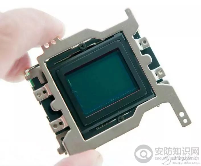
CCD
Charge CoupLED DevICe, which is made of a high-sensitivity semiconductor material that converts light into electric charge and converts it into a digital signal through an analog-to-digital converter chip. The digital signal is compressed and then internalized by the camera. The flash memory or the internal hard disk card is saved, so that the data can be easily transferred to the computer, and the image can be modified as needed and imagined by means of computer processing. A CCD consists of many photosensitive units, usually in megapixels. When the CCD surface is exposed to light, each photosensitive unit reflects the charge on the component, and the signals generated by all the photosensitive units are added together to form a complete picture.
CMOS
Complementary Metal-Oxide SEMIconductor, like CCD, is a semiconductor that can record light changes in digital cameras. CMOS manufacturing technology is no different from general computer chips, mainly using semiconductors made of silicon and germanium, which coexist with N (band-to-electric) and P (with +-electric) levels in CMOS. The semiconductor, the current generated by these two complementary effects can be recorded and interpreted by the processing chip into an image. However, the shortcoming of CMOS is that it is too easy to appear noise, mainly because the early design makes CMOS overheat when the current changes too frequently when dealing with rapidly changing images.
The advantage of CCD is that the image quality is good, but due to the complicated manufacturing process, only a few manufacturers can master it, resulting in high manufacturing costs, especially for large CCDs, which are very expensive. At the same resolution, CMOS is cheaper than CCD, but the quality of the image produced by CMOS devices is lower than that of CCD. So far, the vast majority of consumer grades and high-end digital cameras on the market use CCD as a sensor; CMOS sensors are used as low-end products on some cameras, if any camera manufacturer produces an imaginary head using CCD Sensors, manufacturers will spare no effort to use it as a selling point to publicize, even under the name of "digital camera." For a time, whether or not there is a CCD sensor has become one of the standards for people to judge the grade of digital cameras.
One of the advantages of the CMOS image sensor is that the power consumption is lower than that of the CCD. The CCD provides excellent image quality, and the cost is high power consumption. In order to make the charge transmission smooth and the noise is reduced, the transmission effect needs to be improved by the high voltage difference. . However, the CMOS image sensor converts the charge of each pixel into a voltage, which is amplified before reading, and can be driven by a 3.3V power supply, and the power consumption is lower than that of the CCD. Another advantage of the CMOS image sensor is its high integration with peripheral circuits, which can integrate the ADC and the signal processor to greatly reduce the size.
Noise
Since each photodiode of CMOS needs to be equipped with one amplifier, if it is in megapixels, then more than one million amplifiers are needed. The amplifiers are analog circuits, and it is difficult to make the results of each amplifier consistent, so Compared to a CCD sensor with an amplifier placed at the edge of the chip, the noise of the CMOS sensor increases a lot, affecting image quality.
power consumption
The image acquisition mode of the CMOS sensor is active, and the charge generated by the photodiode is directly amplified by the adjacent transistor; while the CCD sensor is passively collected, the voltage must be applied to move the charge in each pixel to the transmission channel. This applied voltage usually requires 12~18V, so the CCD must have more precise power line design and compressive strength. The high driving voltage makes the CCD consume much more power than CMOS. CMOS consumes only 1/8 to 1/10 of the CCD.
cost
Since the CMOS sensor adopts the most commonly used CMOS process of a semiconductor circuit, it is easy to integrate peripheral circuits (such as AGC, CDS, Timing generator or DSP) into the sensor chip, thereby saving the cost of the peripheral chip; and the CCD adopts charge transfer. The way to transfer data, as long as one of the pixels can not run, will result in a whole row of data can not be transmitted, so the yield of controlling CCD sensor is much more difficult than CMOS sensor, even experienced manufacturers are difficult to come in the half year of the product Within 50% of the level, the manufacturing cost of the CCD sensor will be higher than that of the CMOS sensor.
The prospect of CCD and CMOS sensors is superior to CMOS in terms of image quality, while CMOS has the characteristics of low cost, low power consumption, and high integration. However, with the advancement of CCD and CMOS sensor technology, the difference between the two will gradually decrease. The new generation of CCD sensors has been improving power consumption, while CMOS sensors are lacking in resolution and sensitivity. It is believed that the ever-improving CCD and CMOS sensors will bring us a better world of digital imaging.
Dark current
The dark current is the amount of current released by the photodiode when there is no incident light. The ideal dark current of the image sensor should be zero. However, the actual situation is that the photodiode in each pixel acts as a capacitor at the same time. When the charge is released, even if there is no incident light, the voltage of the dark current is equivalent to the output voltage of the low-intensity incident light. Dark current is one of the factors that affect image quality.
With the rise of digital cameras and mobile phone cameras, image sensors are gradually becoming one of the most dazzling stars in semiconductor products. In image sensors, Japanese-owned CCD sensors and hundreds of contending CMOS sensors are trying to overcome their shortcomings. I hope to become the mainstream technology in the market. In view of this, this article will first introduce the difference in principle between CCD and CMOS sensors, and then explore the blueprint of the technology development of leading manufacturers to understand the development trend of these different image sensors in the application market.
Difference between CCD and CMOS sensor technology
CCD and CMOS sensors are two image sensors that are currently widely used. Both use photodiodes for photoelectric conversion to convert images into digital data. The main difference is that digital data is transmitted in different ways.
The charge data of each pixel in each row of the CCD sensor is sequentially transferred to the next pixel, outputted by the bottommost portion, and amplified by the amplifier at the edge of the sensor; and in the CMOS sensor, each pixel It will be adjacent to an amplifier and A/D conversion circuit, and output data in a manner similar to a memory circuit.
The reason for this difference is that the special process of CCD can ensure that the data will not be distorted during transmission, so the data of each pixel can be concentrated to the edge and then amplified; while the data of CMOS process will be generated when the transmission distance is long. Noise, therefore, you must first zoom in and then integrate the data of each pixel.
Due to the different ways of data transmission, there are many differences in performance and application between CCD and CMOS sensors. These differences include:
1 sensitivity difference
Since each pixel of the CMOS sensor is composed of four transistors and one photodiode (including an amplifier and an A/D conversion circuit), the photosensitive area of ​​each pixel is much smaller than the surface area of ​​the pixel itself, and thus the pixel size is the same. In case of CMOS sensor, the sensitivity of the CMOS sensor is lower than that of the CCD sensor.
2 cost difference
Since the CMOS sensor adopts the most commonly used CMOS process of a semiconductor circuit, it is easy to integrate peripheral circuits (such as AGC, CDS, Timing generator, or DSP) into the sensor chip, thereby saving the cost of the peripheral chip; Since the CCD transmits data by means of charge transfer, as long as one of the pixels cannot be operated, a whole row of data cannot be transmitted. Therefore, the yield of controlling the CCD sensor is much more difficult than that of the CMOS sensor, even if there is an experienced manufacturer. It is difficult to break the 50% level within half a year of the product launch, so the cost of the CCD sensor will be higher than the CMOS sensor.
3 resolution difference
As mentioned above, each pixel of a CMOS sensor is more complex than a CCD sensor, and its pixel size is difficult to reach the level of the CCD sensor. Therefore, when we compare CCD and CMOS sensors of the same size, the resolution of the CCD sensor is usually Better than the level of CMOS sensors. For example, CMOS sensors on the market today can reach a level of up to 2.1 million pixels (OmniVision's OV2610, introduced in June 2002), which measures 1/2 inch and has a pixel size of 4.25μm, but Sony in December 2002. Introduced the ICX452, which is about the same size as the OV2610 (1/1.8-inch), but with a resolution of 5.13 million pixels and a pixel size of 2.78 mm.
4 noise difference
Since each photodiode of a CMOS sensor needs to be matched with an amplifier, and the amplifier is an analog circuit, it is difficult to make the result of each amplifier consistent, so compared with a CCD sensor with only one amplifier placed at the edge of the chip, the CMOS sensor The noise will increase a lot and affect the image quality.
5 power consumption difference
The image acquisition method of the CMOS sensor is active, and the charge generated by the photodiode is directly amplified by the transistor, but the CCD sensor is passively collected, and an external voltage is required to cause the charge in each pixel to move, and in addition, the voltage is usually required to be reached. 12~18V; therefore, in addition to the difficulty in designing the power management circuit (the power IC is required), the high driving voltage makes the power consumption much higher than that of the CMOS sensor. For example, OmniVision's recently introduced OV7640 (1/4", VGA) runs at 30 FPs and consumes only 40mW; Sanyo, which is dedicated to low-power CCD sensors, introduced 1/7" last year. The CIF-rated products still have a power consumption of more than 90mW. Although the company will launch a new 35mW product in the near future, it still has a gap with the CMOS sensor and is still in the sample stage.
In summary
CCD sensors are superior to CMOS sensors in terms of sensitivity, resolution, and noise control, while CMOS sensors are characterized by low cost, low power consumption, and high integration. However, with the advancement of CCD and CMOS sensor technology, the difference between the two has gradually narrowed. For example, CCD sensors have been improved in power consumption for the mobile communication market (the representative in this regard is Sanyo); CMOS sensors are lacking in resolution and sensitivity for higher-end image products. We can see some clues from the product planning of the following major vendors.
Capacitor Motor,Furnace Capacitor,Start Capacitor,Capacitor Start Motor
Wentelon Micro-Motor Co.,Ltd. , https://www.wentelon.com