
Digital circuit level standard full resolution
Input: VIH>3.5V, VIL<1.5V.
It can be seen that the noise margin of the TTL level is 0.4V, and the noise margin of the CMOS is 1.5V.
TTL and CMOS gate structure:
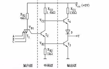
As shown in the TTL gate structure, the output stage uses a push-pull output structure, and T4 is in the form of an emitter follower. The output resistance is small and the load capacity is strong.
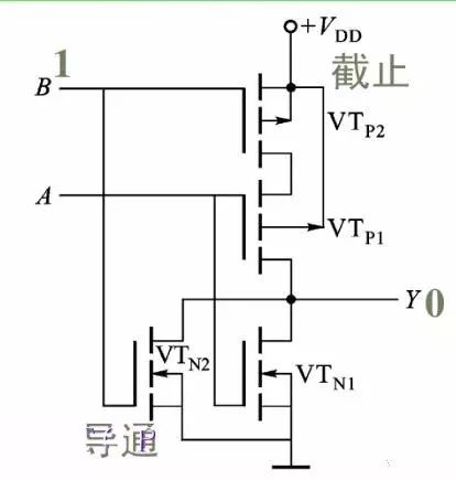
As shown in the CMOS gate structure.
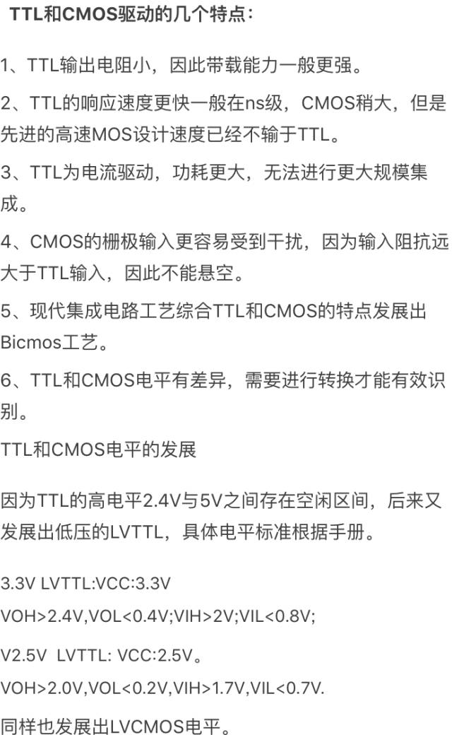
3.3V LVCMOS: Vcc: 3.3V; VOH>=3.2V; VOL<=0.1V; VIH>=2.0V; VIL<=0.7V. 2.5V LVCMOS: Vcc: 2.5V; VOH>=2V; VOL<=0.1V; VIH>=1.7V; VIL<=0.7V.
Second, high-speed level standardsHow to achieve high-speed drive output in high-speed circuits? Either increase the drive current, either lower the level standard or increase the transistor operating speed. Obviously the former will bring very large power consumption, so changing the level standard and improving the transistor design becomes an option. Although the low level is more susceptible to interference, a stricter hardware design is required.
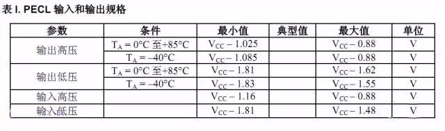
1, ECL and PECL level interface
ECL, Emitter Coupled Logic, uses a differential structure output and requires a negative supply. Later, the development of PECL, that is, positive power emitter coupling logic. The basic principle is to use the transistor to work in the unsaturated zone to reduce the conversion time and greatly improve the conversion speed.
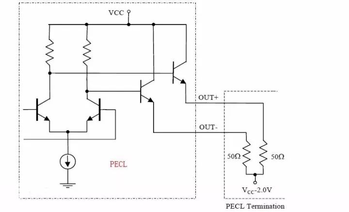
The output of the ECL always has current through it, which is very beneficial for high speed conversion. The output impedance is a few ohms, the output current is about 10 mA, and the driving capability is strong.
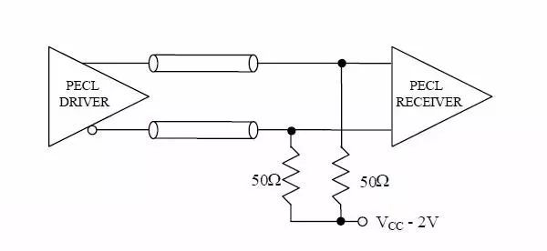
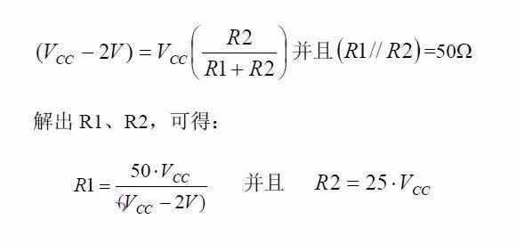
Interface connection: DC coupling, suitable for short distances
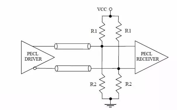
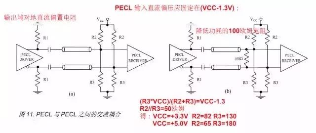
This matching method is equivalent, and the specific resistance is calculated:
Interface connection: AC coupling, suitable for longer distances
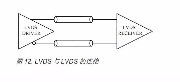
2, LVDS level interface
LVDS, Low-Voltage Differential Signaling, is a level standard for transmitting high-speed signals using low-voltage differential signals. Features: low voltage, low power consumption, strong noise suppression.
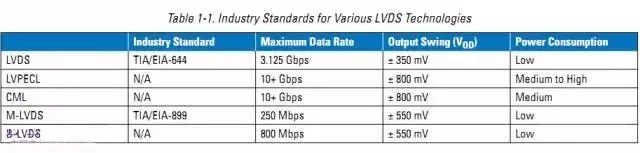
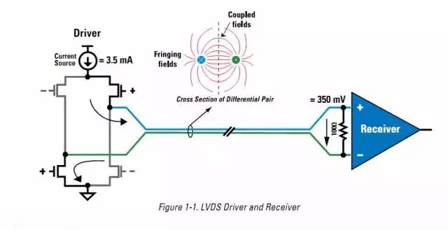
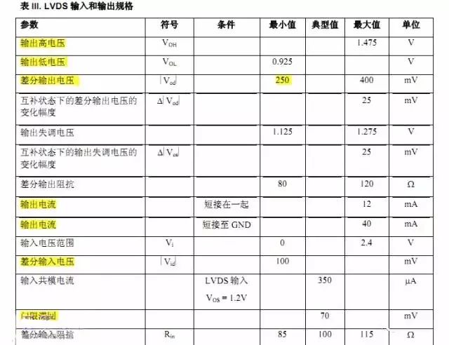
Figure LVDS input and output specifications:
LVDS connection method: direct connection, because there is a termination resistor in the chip.
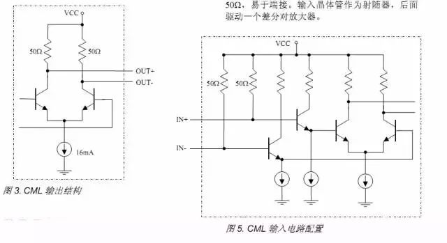
CML is the current mode logic level, which uses constant current drive and built-in matching resistor. It is easy to use and has the longest range of short-distance high-speed applications.
The following figure is a simple comparison of the performance of several high-speed interfaces:


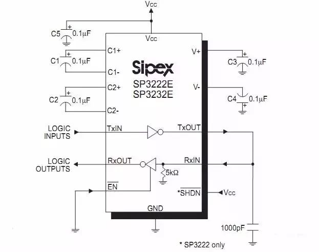
The most widely used in the industrial field should be the 485 232 level standard. Both have advantages and disadvantages, low cost and simple use, but there are still many technical points that can be discussed, such as transmission speed, distance, protection design and so on.

RS232 and RS485 connection problems:
At work, I learned that many students have been confused about the connection of 232 or 485. Regarding the definition of the transceiver and the connection of the male and female heads, I often felt puzzled at first. The main line is to send and receive the three lines.
The standard 232 is the DB9 connector:
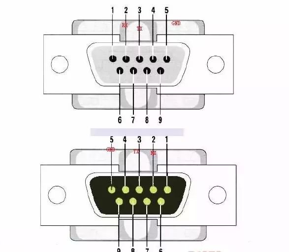
A brief note is: 235-receiving land.
485 how to use DB9 connection:
The two lines of 485 correspond to the 1, 2 feet of the DB9 head.
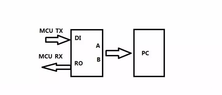
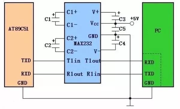
232 and 485 connections to the MCU:
There are mainly several standards for digital levels. These are defined at the hardware level. In software, there are various protocols for communication methods. The interface design is indeed the focus of circuit design, especially in the current high-speed digital communication applications, I think there are several main aspects to be mastered:
1. The application circuit of the signal level, that is, the basic structure should be clear.
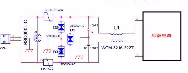
2, protection design issues should be considered comprehensively, different interfaces for load requirements for matching degrees are not the same.
3, the importance of PCB design, in the high-speed design, many use EDA software simulation to help find the problem of interference, but the first thing to do is to strictly follow the relevant rules and specifications to design.
4. The necessity of the experiment. Especially for the interference problem of the interface, the most comprehensive experimental design is one of the best ways to solve the problem as soon as possible.
In short, the theoretical basis must be, design considerations must be, test experiments must be full, and so, the results may be good!
Fiber Pen Nib,Passive Capacitive Stylus Pen,Rubber Tip Stylus Pen,Microsoft Stylus Pen
Shenzhen Ruidian Technology CO., Ltd , https://www.wisonens.com