
Load image visualization is an important requirement in deep space exploration missions. However, due to the limitation of channel bandwidth, all payload data cannot be transmitted in real time. Therefore, the extraction and transmission of images in spaceborne multiplexed memory is the key to realize task visualization.
In this paper, a load image extraction method is designed, which is suitable for space-borne exploration spacecraft load self-management and visualization applications. Image frame frame playback algorithm is realized by image frame recognition, pointer management and data filtering, which has the characteristics of complete image, real-time and rate adaptive. The method is implemented by FPGA in a certain detector engineering project, and has been tested and tested to meet the requirements of engineering visualization.
0 Preface
With the development of deep space exploration mission requirements, the on-board data stream is complicated and diversified, and the demand for on-orbit data processing is growing rapidly. Ground visualization is one of the important requirements of deep space exploration engineering tasks, and the storage of on-orbit images And real-time extraction of the downlink is the key to solving the visualization needs. In actual engineering, there is a contradiction between the amount of image data and the downlink rate. In engineering applications, it is necessary to obtain high-resolution load images, which leads to an increase in data rate. Deep space detection is limited by the distance and rate of the digital transmission channel. Pass all the data. Therefore, it is necessary to process the image in the on-board multiplex memory, store the image data while extracting the entire frame, and down-deliver the latest image to realize the task visualization. The function of the on-board multiplexed memory is to form multiple data streams in different formats of payload data according to the advanced on-orbit system protocol format, and form multiple virtual channel data units (VCDUs) by sharding and framing, and store them in mass storage. The chip (FLASH) simultaneously plays back the data in the large-capacity memory chip according to the selected address, and filters the playback data according to requirements.
Aiming at the above requirements, the load rate adaptive load image extraction method is realized by image frame recognition, pointer management and data filtering in the storage and playback process of the on-board multiplexed memory, and realized and verified by FPGA, which can be used for subsequent deep space detection. The load data management task provides a technical reference.
1 frame playback algorithm
The function of the on-board multiplexed memory is to multiplex the multi-load payload image data, store the multiplexed data stream in the large-capacity memory, read the data in the cache according to the playback command, perform channel coding, and output the data to the digital transmission.
The process of frame-drawing playback should be combined with the working process of the multiplexed memory. Due to the large amount of image data, the multiplexer entry cannot cache the entire image. Therefore, considering the hardware and software overhead, the design marks the data during the recording and extracts Completed during playback after storage.
The extraction method is shown in Figure 1. The image is input in serial form through the LVDS interface. In the interface preprocessing module, an image is sliced ​​and filled into multiple virtual channel data units (VCDUs) for storage and downlink.
At the same time, the head and tail of the image data are determined by using the following gating signal, and an image frame header and a tail end identification signal are generated to identify a complete image. The information appending module organizes the head and tail identification signals into additional information and fills in the data.

In order to ensure that the played back image is always the latest image data, it is necessary to know the frame head VCDU address of the latest image and the storage address of the frame tail VCDU. Therefore, during the recording process, a new image data frame address register is used to record the frame header end VCDU address of the latest image in the memory, and the address information in the latest image data frame address register is updated immediately after each complete image data is received. Ensure that the address in the latest image data frame address register is the frame header end VCDU address of the latest image data.
During playback, the data request signal is received, and the playback control module loads the latest image address from the latest image data frame address register, and plays back from this address until the data frame with the tail frame mark byte is encountered, and an image is extracted. Playback, then continue to load the latest image data frame address register for the next image playback.
Due to the data multiplexing design, multiple images will enter the memory at the same time and exist in the form of multiple VCDUs. The page operation of FLASH causes the data to be played back two VCDUs each time, so the additional information is designed in the alternate symbol domain. The interpretation of the additional information filters out the extra data, ensuring that the playback data is full of valid extracted images.
The rate of playback depends on the rate of the downstream channel, which is controlled by the playback request signal of the upper level in the project. When each request arrives, the latest image address pre-stored is loaded, which not only ensures the real-time performance of the image, but also meets the requirements of the extraction rate adaptation.
The frame-pull playback algorithm mainly considers three aspects: the extracted image is the complete load image data; the currently extracted image is the latest data; the extraction algorithm is adaptive to the extraction rate.
1.1 Integrity design
The input image data is generated by the interface module. The different load data is divided into VCDUs of different classes by VCID. Since the FLASH adopts the page operation mode, the size of one page is 2 KB, and one page of the design contains two VCDUs.
FLASH reads and writes are based on page operations. There are many possibilities for reading two VCDUs in one page. The data processing process is shown in Figure 2. Figure 3 shows three possibilities. The first one is needed. The extracted header data, the latter is the intermediate data that needs to be extracted; the second is the image data that needs to be extracted, the latter one is the other VCDU data that needs to be extracted; the third is the tail data that needs to be extracted, and the latter is The head of the next image, but does not need to be extracted.
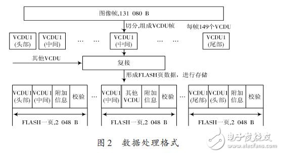
It can be seen that certain data must be filtered out in the extraction and playback to ensure the integrity and correctness of the extracted image, so additional information is added during storage to solve the image integrity problem.
The additional information is designed as 6 b, and the format definition is shown in Table 1.
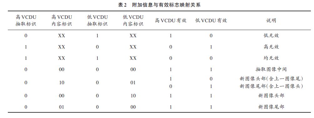
Additional information is stored with the data in the memory chip. At the time of playback, the additional information is read, and the high VCDU valid/invalid signal and the low VCDU valid/invalid signal are parsed. Data filtering by the playback request module ensures that only valid data is played back and is a complete image.
The relationship between the additional information and the valid flag is shown in Table 2. For each case of the input data, the valid/invalid signal is parsed according to the mapping relationship in Table 2.
The data filtering module sets the buffer, controls the cache address according to the high and low VCDU effective flag, reads for 1, and skips invalid VCDU data for 0 to achieve data filtering.
1.2 Real-time design
In the method, the frame header VCDU information and the frame tail VCDU information must be obtained to update the image data frame address register, that is, after a whole image is received, playback can be performed.
The extracted delay calculates the difference between the first bit output and the input time of an image. In the worst case, the Nth image has been written. The N + 1 image is not written at the end, that is, it is written in the Nth image header. The last two images will start playing back. Delay time during extraction = two image times + data playback time. In the project, the image generation rate is 10 frames/s, and the generation time of one image is calculated as 100 ms.
The time for playing back data is the data readout time and data buffer time from the FLASH chip, 2 KB per page, and the read time is about 320 μs; the registration time on the remaining processing paths is 10 μs. Therefore, the delay time during the extraction process is about 200.33 ms, which can fully satisfy the playback viewing needs of images.
1.3 Rate Adaptive Design
The ratio of image extraction (ie, the interval at which the image is extracted) is related to the input rate and playback rate. In engineering applications, the input image rate is 13.33 Mb/s and the playback rate is 50 Kb/s, where the image effective data rate is 41.808 Kb/ s, an image size of 131 080 B, each image forms 149 VCDU frames, a total of 149 & TImes; 1 024 B = 152 576 B.
Playback at a rate of 50 Kb/s, playback of an image requires 152 576 & TImes; 8/41 808 = 29.19 s, during which the image 29.19 & TImes; 10 = 291.9, about 292 frames, that is, an image of about 292 frames is taken. .
The key to achieving rate adaptation is that the various steps of the extraction method are not coupled to the input rate and playback rate.
The input data is identified by the beginning and end of the frame, and is divided into VCDUs that identify the head and tail. The input data rate changes, which only affects the data interval of the VCDU.
The data interval of the VCDU actually affects how often the write control module operates on the FLASH chip. Therefore, when the input rate meets the entry rate requirements, the data can be stored normally and additional information is generated, and the input rate has no effect on the method.
After the playback data is read from the FLASH, the additional information is parsed, buffered, and the invalid data is filtered out and output and played back. A change in the playback rate will cause the interval of the playback control module to load the head and tail registers to change. The playback rate is slowed down, the load interval is increased, and the head and tail address registers are refreshed multiple times by the write control module, that is, the interval at which the image is extracted is automatically increased. The playback rate is increased and the load interval is reduced. Since the playback module can correctly load the new address when the algorithm considers that only the new header and tail addresses are stored, the playback module will stop waiting for the new image at the current address. Therefore, the interval for extracting images is automatically reduced. When there is no new image, the extraction module waits for new data to enter.
The adaptive rate is beneficial to the stability and versatility of the algorithm. The input and playback rates can be changed without changing the extraction program.
Solar Post Top Lights save money and inspire your home at the same time. Solar Post Cap Lights are rigid black plastic caps with a solar panel.The extremely efficient LED battery produces white accent lighting for 12 hours.Post Top Light Fixture is brighter than most rivals and comes in various style such as downward-facing post, upward-facing light and more industrial
Solar Post Top Lights
Solar Post Top Lights,Solar Post Cap Lights,Post Top Light Fixture,Post Top Fixtures
Shenzhen Bbier Lighting Co., Ltd , https://www.chinabbier.com