
When Edison invented the light bulb, it failed more than 8,000 times. Someone ridiculed him and said: "You have failed more than 8,000 times, it's amazing!" Edison said calmly: "Sir, you are wrong, I just proved that more than 7,600 materials are not suitable for filaments." After the failure, Edison finally achieved success and became a world-famous person.
Indeed, there are many "smart" people in the world who hope to obtain shortcuts to success from others, hoping to bypass the more than 8,000 failures and directly achieve peer-to-peer success. I have never used Edison's thinking mode to realize that success is a road that is constantly being tried. Success is a process from 0 to 1. Today, let us review the top ten technological revolutions in the 3D printing industry in the first half of 2016. (No matter the ranking)
INNOVATION1: Swiss scientists 3D printing gold and silver nano wall can produce higher performance touch screen
Touch screen technology is achieved by means of tiny conductive electrodes that are sprayed onto the surface of the device. This electrode, which is almost invisible to the naked eye, is composed of nano-walls made of a conductive material, and the most commonly used material is indium tin oxide. Its transparency is high, but its conductivity is poor. The Zurich Federal Institute of Technology (ETH) has found a viable and innovative approach – “nanodroplet†3D printing. This method can print ultra-thin “nano wall†with gold and silver nanoparticles as raw materials, thus creating transparent conductive electrodes that have never been seen before, and finally creating a touch screen with better picture quality and more accurate response. The new method of ETH - using gold and silver nanoparticles as raw material 3D printed nano wall has no such defect, because it can achieve high transparency and conductivity at the same time.
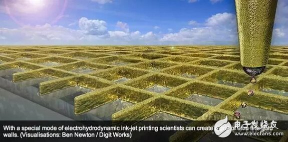
The magic of ETH's nano 3D printing technology not only allows metal materials to maintain their original conductivity, but also creates transparent structures. At present, researchers have used this technology to successfully print 3D ultra-thin electrode layers with thickness between 80-500 nm.
INNOVATION2: From resin to ceramics, California high temperature ceramic 3D printing technology
The HRL lab in Malibu, Calif., invented a compatible resin formulation for photocuring/3D printing that can be fired to produce dense ceramic parts after 3D printing. This is an amazing breakthrough because it enables the production of arbitrary polygonal ceramic parts that are strong and temperature-free, without any machining of the ceramic surface, without the need for casting or caulking.
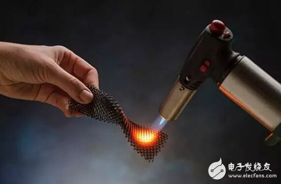
HRL Precursable monoomers—“precursor-converting polymers†that rapidly shape ceramics by UV light curing. Ceramics made from these polymers shrink uniformly and have almost no porosity. Mini-grid and honeycomb materials can be formed, which are not only complex in shape but also high in strength. Such density foam ceramics can be used in propulsion parts, thermal protection systems, porous burners, MEMS and electronic equipment. When used in hypersonic vehicles and jet engines, this ceramic can help designers create small parts that resist heat and high temperatures caused by exhaust gases from the takeoff process.
I NNOVATION3: 1000 times faster than existing systems, MIT will redefine 3D scanning
Most Lidar systems currently on the market (including those installed on self-driving cars) use discrete free-space optics, including lasers, lenses, and external receivers. In these hardware combinations, the laser rotates while oscillating, which limits its scanning range and complexity. And the cost ranges from $1,000 to $70,000.
MIT's lidar chips are smaller, lighter, cheaper, and potentially more powerful, because there are no moving parts in the chip, and the speed is 1000 times faster than current lidar systems, which can be used to track high-speed moving vehicles. .
The MIT laser radar chip works closely with silicon photonics. The wavelength of the silicon waveguide is much smaller than that of the fiber, which makes the photonic circuit on a very small chip have properties similar to optical fibers. The technology is also not expensive to commercialize and can be produced in a large number of CMOS foundries and addresses issues such as waveguide loss and optical isolation.
Solar lighting systems use solar cells to convert solar energy in nature into electricity and provide it to LED light sources. Due to the low voltage, energy saving and long-term characteristics of LED light sources, the application of solar LED lighting systems will achieve high energy efficiency, reliability, and practical value.
Solar panels are used to receive solar radiation during the day and convert light energy intoelectrical energy stored in the storage battery by controller while the battery starts discharging and illuminate the light source in the evening. In the morning, the controller will switch off the battery and stop discharging according to the illuminance. The main function of the controller is to control the street lamp switch, adjust the brightness, and protect the battery to prolong the service life.
Solar Lights,Solar Lights, Led Lights, Garden Decoration, Led Street Lights, Led Lamp
Wuxi Sunket New Energy Technology Co.,Ltd , https://www.sunketsolar.com