In the early development of integrated optics, Tian Binggeng once made three definitions of integrated optics: (1) Optical waveguides can restrict the propagation of light beams. (2) Various optical waveguide devices can be made using optical waveguides; (3) Integrating optical waveguides and optical waveguide devices can form an integrated optical path with specific functions. Integrated optics has taken fiber optic communication as one of its main application goals from the beginning.
With the rise and development of optical fiber communications, integrated optical devices have gone through decades. Integrated optical devices not only become an important part of the optical fiber network, but also promote the explosive growth of optical fiber communication capacity, the rapid development of optical fiber communication technology and industry, coupled with the further development and maturity of integrated optical device technology will also set off optical fiber communication technology and related New climax of industrial development.
development path
Integrated optics is based on the principle that thin films can transmit electromagnetic energy in the optical frequency band. Therefore, its birth is mainly affected by microwave engineering and thin film optics. Before 1962, planar dielectric waveguides have been used in microwave engineering, but it was not until 1965 that Anderson and his research team combined microwave theory and lithography to produce thin-film waveguides and other planar devices for the infrared region. Light path. In 1969, SE Miller of Bell Labs first proposed the concept of "integrated optics" (integrated opTIcs), announcing the beginning of vigorous research and development of perfect and reliable thin film technology for optical communications.
In the early 1970s, researchers made a lot of research on the materials and manufacturing process of making waveguides. During this period, great progress has been made in the manufacture of light-emitting diodes (LEDs), laser diodes (LDs), and optical fibers. The reduction of optical fiber propagation loss has accelerated the development of optical fiber communication systems. In the late 1970s, technologies related to optical fiber communications were further mature, and enterprises and research institutions began to focus on the development of optical fiber communication systems; instead, research on integrated optics was reduced. They believed that commercialization of integrated optical devices would be difficult to achieve in the near future. In the 1980s, researchers began to refocus on the development of integrated optics because discrete components in fiber optic communication systems are difficult to collimate and their performance is not stable enough.
Classification of planar optical waveguide devices
Optical waveguide is an important basic component of integrated optics, which can confine the optical beam in the medium of the size of the optical wavelength. For various planar optical waveguide devices made by integrated optical technology, some electrodes are also deposited at a certain position, and a voltage is connected at both ends to control the phase or intensity of the light wave transmitted in the waveguide. Then, the optical waveguide is coupled with the optical fiber or the optical fiber array. The laser signal is coupled, transmitted, and modulated in the optical waveguide.
Optical waveguide devices can be divided into four basic types according to their constituent materials: lithium niobate titanium-coated optical waveguides, silicon-based silicon dioxide optical waveguides, InGaAsP / InP optical waveguides, and polymer optical waveguides.
The electro-optical, acousto-optical and nonlinear optical coefficients of LiNbO3 crystal are large, and the chemical properties of the material are stable. The crystal growth cost is low and it is easy to grow a large size single crystal, which is suitable for making various modulation, coupling and transmission elements, but it cannot be used as a light source and a detector. It is the most commonly used crystalline material for integrated optics.
The main process of lithium niobate titanium-coated optical waveguide is: firstly, a titanium film is deposited on the lithium niobate substrate by evaporation or sputtering deposition, and then photolithography is performed to form the desired optical waveguide pattern, and then diffusion is performed. It can be achieved by external diffusion, internal diffusion, proton exchange and ion implantation. Finally, a silicon dioxide protective layer is deposited to make a planar optical waveguide. The loss of this waveguide is generally 0.2-0.5dB / cm; the driving voltage of the modulator and switch is generally about 10V; the bandwidth of the general modulator is several GHz, and the LiNbO3 optical waveguide modulator using the traveling wave electrode has a bandwidth of 50GHz the above.
The current research on LiNbO3 optical waveguide devices is mainly to further improve the working rate of LiNbO3 modulators and develop LiNbO3 devices and integrated modules with other functions, such as TI: Er: LiNbO3 lasers, doped Er optical waveguide amplifiers and LiNbO3 optical waveguide switches Wait.
Silicon-based silicon dioxide optical waveguide is a new technology developed in the 1990s. For its production, a thicker silicon dioxide layer needs to be deposited, and the refractive index of the film layer can be adjusted by adding a dopant such as germanium or by adding nitrogen to generate nitrogen oxide. You can also add other substances to the oxide, such as adding boron and phosphorus to produce borophosphosilicate glass (BPSG).
This technology is relatively mature abroad. Its manufacturing processes are: flame hydrolysis method (FHD), chemical vapor deposition method (CVD, developed by NEC), plasma enhanced CVD method (FECVD, developed by Lucent), reactive ion etching technology (RIE), porous silicon oxidation method and Sol-gel method (Sol-gel). The loss of this waveguide is very small, about 0.02dB / cm.
InGaAsP / InP optical waveguides based on indium phosphide (InP) can be integrated on the same substrate with InP-based active and passive optical devices and InP-based microelectronic circuits, but their coupling losses with optical fibers are large.
The thermo-optic coefficient and electro-optic coefficient of the polymer waveguide are relatively large, which is very suitable for the development of high-speed optical waveguide switches and AWG. The polymer material can be deposited on any semiconductor material, which provides convenience for manufacturing the electro-optic modulator. In addition, due to the low relative dielectric constant of the polymer, it provides convenience for making high-speed broadband traveling wave structures. Since the preparation process of the organic polymer is compatible with the semiconductor, the preparation of the device is very simple. The AWG developed by Germany's HHI company using this waveguide has a wavelength drift of only ± 0.05nm at 25-65 ℃.
It should be pointed out that among the above-mentioned four planar optical waveguide devices, except for the LiNbO3 planar optical waveguide device, the remaining three optical waveguide devices are not yet mature and are still in the research and development stage.
Integrated optical device for optical fiber communication
At present, the most used integrated optical devices in optical fiber communication are: optical couplers (Coupler, Splitter), optical modulators, optical switches, tunable optical filters (OTF), etc.
Optocoupler
An optical coupler is a functional device that realizes optical signal splitting / combining, and generally splits and combines optical power of the same wavelength. The couplers used for optical fiber communication are divided into: optical fiber fused-cone coupler, micro-electromechanical element type (MEMS) coupler and integrated optical waveguide type coupler. The integrated optical waveguide coupler is introduced here.
Planar optical waveguide technology can be used to make integrated optical waveguide couplers with different structures and functions. The main processes are: deposition, lithography, and diffusion. Figure 1 shows the basic structure of the simplest Y-shaped (1 & TImes; 2) branch coupler.
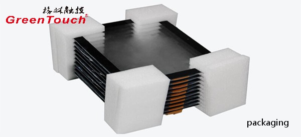
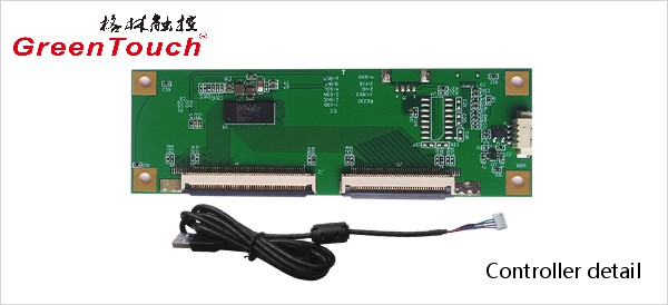
This product response time is shorter than resistive tonch screen's with a good touch.It is widely used to Phone,Tablet,E-book,gaming device by hands holding,Touch Monitor,GPS,All-In-One and so on.GreenTouch projected capacitive touch technology is with fast and sensitive response, the design with frame (without frame is optional) makes it looks professional and generous. The model is designed for high-intensity and high-frequency business environments.
Product show:
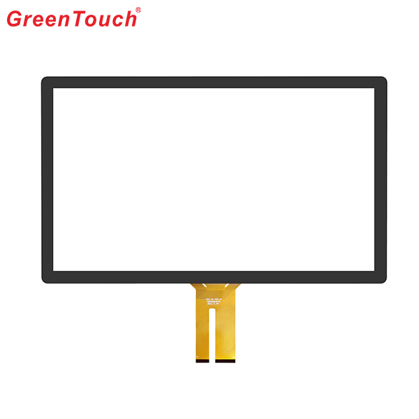
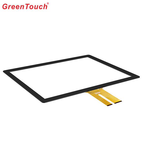
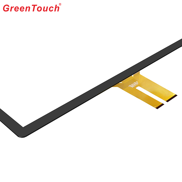
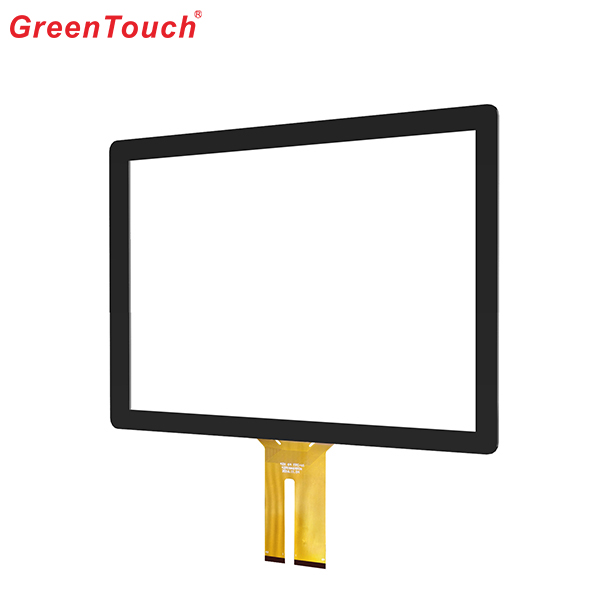
Capacitive Touch Screen Panel,Android Touch Screen,Portable Touch Screen,Pcap Touch Screen,POS Terminal Touch Screen,Mini Capacitive Touch Screen
ShenZhen GreenTouch Technology Co.,Ltd , https://www.bbstouch.com
