
0 Preface
With the rapid development of integrated technology, portable communication devices with small size have a broader market prospect. But there are stricter requirements for the audio power amplifier chips used in these portable devices. Portable devices are small and powered by batteries, so audio power amplifier chips are required to have as few peripheral devices as possible and consume as little power as possible. In addition, for communication equipment, CDMA noise is generated at a frequency of 217 Hz, so the audio power amplifier must also have a strong power supply rejection ratio (PSRR). The audio power amplifier in this article is specifically designed to provide high-quality output power with as few external components as possible. It does not require external bootstrap capacitors and coupling capacitors, so it is very suitable for mobile phones or other low-voltage devices.
l Circuit structure design is well known. Class AB amplifiers have higher efficiency than Class A amplifiers and lower crossover distortion than Class B amplifiers. It is now the main force in the audio power amplifier market. The output op amp is the core of the entire circuit, and its performance directly affects the performance parameters of the entire chip.
1.1 The choice of op amp structure
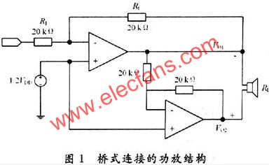
In this paper, two op-amps with Class AB output are used to form a bridge structure, as shown in Figure 1. The gain of the first amplifier can be set externally, while the gain of the second amplifier is a unity gain fixed internally. The closed-loop gain of the first amplifier is determined by the ratio of Rf and RI, and the gain of the second amplifier is fixed by two internal 20 kΩ resistors. As can be seen in Figure 1, the output of the first amplifier serves as the input of the second amplifier, so that the outputs of the two amplifiers are equal in amplitude and 180 ° out of phase. Therefore, the differential gain of the entire circuit is: 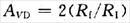
The operation of the bridge structure is different from the classic single-ended output amplifier structure with the other end of the load grounded. Compared with amplifiers of single-ended structure, the design of bridge structure has its unique advantages. It can drive the load differentially, so the output voltage swing can be doubled when the operating voltage is fixed. Under the same conditions, the output power is 4 times that of the single-ended structure. The bridge structure has another advantage over the single-ended structure. Because it is a differential output, Vo1 and Vo2 are biased at 1 / 2VDD, so there is no DC voltage on the load. This eliminates the need for output coupling capacitors, which is necessary in single-supply single-ended output amplifiers. Without output coupling capacitors, a 1 / 2VDD bias on the load can cause power consumption and possible loudness within the integrated circuit loss. In view of the above advantages, the circuit structure selected here is a bridge-connected amplifier structure consisting of two Class AB output op amps.
1. 2 amplifier circuit structure
The amplifier circuit diagram is shown in Figure 2. The first stage of the amplifier is a folded cascode structure, which improves the common-mode input range and power supply noise suppression characteristics of the two-stage operational amplifier. It can be seen as a structure in which a differential transconductance stage and a current stage are cascaded followed by a Cascode current mirror load. The second stage is a class AB push-pull output, which can efficiently use the supply voltage and supply current. The difference from the common cascode amplifier is that four tubes M11, M12, M13, and M14 are added to the output end, making the single-ended output into a double-ended output. These four tubes together with the bias circuit and the second-stage push-pull output circuit form two transconductance loops.
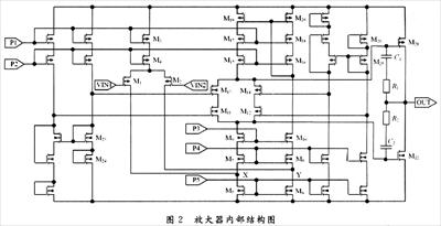
A transconductance loop is a circuit that provides a linear relationship through a nonlinear circuit. In Figure 2, M21, M13, M23, M24 and M22, M12, M25, M26 each form a trans-conductor loop, which is easy to obtain: 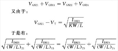
As a result, a current expression related to the size of the transistor is obtained. It can be seen from the formula that the quiescent current of the output power tube M21 is determined by the width and length ratios of M13, M21, M23, and M24 and the current, and has nothing to do with the input signal. Therefore, the width-to-length ratio of the four tubes is set in advance, and a fixed current is given to M13, M23, M24, and the static current of the output power tube is determined. But whether adding four MOS tubes to the op amp will not affect the other performance of the op amp. From the perspective of the signal path, only DC current flows through the transistors M11, M12, M13, and M14, and no AC current passes through them. They shield the AC behavior and present an infinite AC impedance to the current from the first stage. These four MOS tubes set the quiescent current of the output power tube, but they have no effect on the gain and bandwidth of the first stage. So the gain of the amplifier is still: 
The purpose of using a transconductance loop is to prevent one output transistor from turning off when a large current flows through one output transistor. In fact, when M21 flows a large output current, M22 may be turned off. In the case of a large output current, at least a minimum current must flow through M22, which can reduce crossover distortion and increase speed.
For such a multi-pole two-stage op amp, Miller compensation is done in series with the output resistance and capacitor to increase the phase margin and improve stability. Through frequency compensation, the two main poles are: 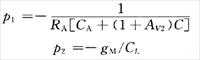
Where: RA is the total impedance from the drain of M9 to ground; CA is the total parasitic capacitance from the drain of M9 to ground; CL is the total capacitance of the output. p1 is the pole generated at the output of the first-stage amplifier. After Miller compensation, it is closest to the origin and becomes the main pole; p2 is the pole generated at the output. Miller is far from the origin after compensation. At the same time, due to the formation of a path by the resistance and capacitance, a zero point is generated: 
Properly adjust R so that z = p2 can make the zero point and the second main pole cancel each other, increasing the stability of the system.
2 Simulation results and analysis
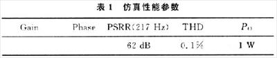
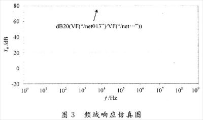
The simulation performance parameters are shown in Table 1. Use Cadence Spectre for simulation. The N-well CMOS process model of China Resources Shanghua 0.5 μm was used, and the simulation environment was VDD = 5 V, T = 27 ℃ typical conditions. Drive an 8 Ω load with a single 5 V power supply. For a 1 kHz, 4 V peak-to-peak sine wave excitation, the simulation shows that the amplitude of the voltage fundamental on the load is 3.9 l V. At this time, the average power consumed by the power supply is 3.15 W, and the efficiency of the power amplifier is 60.7%. The total harmonic distortion is 0.098%. In general, THD and efficiency increase as the input voltage becomes larger. The frequency domain response of the amplifier is shown in Figure 3.
3 Conclusion The AB power amplifier circuit of this design uses a folding cascode structure, a power tube push-pull output, and uses an external current source to supply power, and uses a low-voltage cascode current mirror structure bias circuit. The simulation structure shows that the op amp has the characteristics of high gain, low input offset voltage, low THD, etc. At the same time, it has good frequency characteristics and low static power consumption, which meets the requirements of a high-performance class AB audio power amplifier chip.
Active Linear Array Loudspeaker
Line Array Sound System,Line Array Speaker System,Line Array Loudspeaker System,Active Linear Array Loudspeaker
The ASI Audio Technology Co., Ltd , https://www.asi-sound.com