
For some applications such as communication devices or others, the millimeter wave band is very attractive because of the very wide available band resources from 30 GHz to 300 GHz. But looking for high performance and low cost printed circuit board (PCB) materials in this band is a huge challenge. However, by understanding the key parameters and characteristics of PCB materials in the millimeter wave band, such as the influence of different PCB materials on the performance of different circuits, it is entirely possible to find PCB materials suitable for applications in this frequency band.
There are many factors that need to be considered when designing a microwave circuit. These factors often make circuit design difficult or have a huge impact on the circuit. These factors include suppressing spurious mode transmission, reducing conductor loss and radiation loss, achieving effective signal transitions, reducing interference resonance, and controlling dispersion.
Figure 1a. Microstrip transmission line circuit
Figure 1b. Grounded coplanar waveguide transmission line
Design guideThere are many design methods that can reduce some of the problems in wave transmission, such as the use of very thin circuit substrates. In general, the thickness of the laminate used is less than a quarter of the wavelength of the circuit's highest operating frequency. However, in practical applications, in order to reduce the coupling resonance interference between different circuits in the circuit board, the thickness of the circuit substrate used is preferably lower than one eighth of the maximum operating frequency of the circuit. Not only does the mutual coupling or resonance of the circuit interfere with the transmission of the main signal, but the surface wave generated by it also affects the transmission of the main signal. The width of the signal conductor is related to the thickness of the circuit laminate. The thinner the laminate, the smaller the corresponding conductor width should be. In order to effectively suppress the stray mode, the conductor width should also not exceed one-eighth of the maximum operating frequency of the circuit.
The above laminate thickness and conductor width design methods can be directly applied to high frequency microstrip line circuit design, and other types of circuit design need to consider more factors. For grounded coplanar waveguides (GCPW), also known as metal backplane coplanar waveguides (CPCBW), thicker circuit laminates in the millimeter wave band appear to be advantageous for suppressing spurious mode transmission.
As shown in the microstrip line structure shown in FIG. 1a, there is a certain interval (substrate thickness) between the signal layer and the ground plane in the microstrip transmission line. If the interval is a quarter wavelength, resonance occurs between the two copper foil planes and interferes with the main signal transmission. If the substrate thickness is a quarter wavelength but the copper conductor width is less than or equal to a quarter wavelength, resonance may not occur or may be ignored. If both the substrate thickness and the copper conductor width are greater than or equal to a quarter wavelength, the circuit can easily generate additional resonance and spurious modes. Figure 1b shows a grounded coplanar waveguide structure. Even if the GCPW substrate thickness and conductor width are equal to a quarter wavelength, circuit stray resonance can be avoided due to the coplanar grounded tight coupling structure. The coplanar ground plane is adjacent to the signal conductor and is connected to the ground floor by plated through holes (PTHs). Of course, all the choices of high-frequency circuit structure will have trade-offs in various aspects. For example, the conductor loss of the GCPW circuit is higher than that of the microstrip line circuit. However, considering the operating frequency, since the GCPW circuit has lower radiation loss than the microstrip line circuit, the total insertion loss is not necessarily higher.
For high-frequency transmission lines and high-frequency circuits, insertion loss is the sum of many loss components, including dielectric loss, conductor loss, radiation loss, and leakage loss. High frequency PCB materials generally have large bulk resistance and therefore RF leakage losses are very small. The dielectric loss is related to the loss factor or tan δ of the circuit material. Losses are also affected by other additional materials, such as solder mask inks or bonding sheets. Since the solder resist ink is a high loss material with a loss factor of 0.02, solder resist ink is usually not used in the RF/microwave band, especially in the millimeter wave band. In addition, the influence of the solder resist ink on the dielectric constant (Dk) is difficult to control, and the use of solder resist ink causes impedance mismatch, which further causes an increase in return loss and insertion loss.
Thickness changeSolder mask inks typically have thickness differences between different circuits or even in the same circuit, which can result in unpredictable impedance changes in the circuit. Moreover, solder resist inks generally have a high water absorption rate, which can seriously degrade the performance of the PCB circuit. The dielectric constant Dk of water is 70 and has a much larger loss factor than the circuit material. When the circuit absorbs a certain amount of moisture, the Dk of the circuit material will become larger and the loss of the circuit will also rise. Therefore, use as little or no solder mask ink as possible in the millimeter wave band.
The thinner the substrate used in the circuit, especially the millimeter wave circuit, the greater the conductor loss will become, and the conductor loss will increase significantly with increasing frequency. Usually, during the processing of the PCB substrate, the surface of the copper foil is roughened to improve the bonding rate with the PCB dielectric material. But rough copper foil surfaces can cause higher losses. In general, when the skin depth corresponding to the operating frequency of the circuit is less than or equal to the surface roughness of the copper foil, the influence of the surface roughness will become very significant. In the millimeter wave band, the skin depth is usually less than the surface roughness of the copper foil.
Copper foil surface roughness has a variety of measurement methods and units of measurement. For RF/microwave applications, Rq or root mean square (RMS) measurements are a suitable method of roughness measurement. Table 1a lists the different types of copper foil roughness commonly used in high frequency PCB materials. Table 1b shows that in the millimeter wave band, the skin depth is even comparable to the smoothest copper foil surface roughness.
From the data in Table 1, it is known that circuit designers with applications less than 50 GHz may find that any type of copper has little effect on the circuit because all copper foil types have a surface roughness greater than the skin depth. There are certain errors in this conclusion. Because the rougher surface will produce more parasitic inductance, and the rough surface will cause changes in surface impedance and increase insertion loss. The results of the study shown in Figure 2 show the effect of copper foil roughness on propagation constant and insertion loss.
Copper foil surface roughness
RMS (micron)
Calendered copper 0.3
Low roughness electrolytic copper 0.6
Standard electrolytic copper 1.2
High roughness electrolytic copper 2.4
Table 1a. Surface roughness values ​​of typical copper foils commonly used in RF/microwave circuits
Frequency (GHz) signal in the conductor
Skin depth (micron)
12.00
100.67
500.30
770.24
1100.20
Table 1.b Skin depth of signal at different frequencies
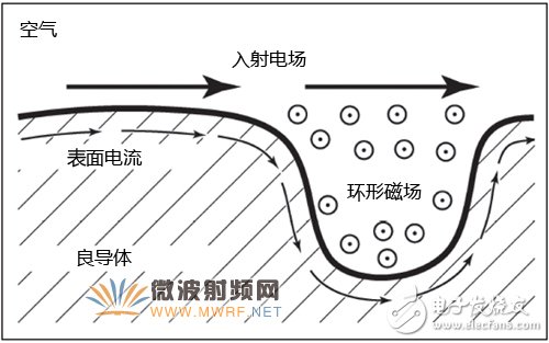
Figure 2. Schematic diagram of the effect of copper foil surface roughness on transmission constant and insertion loss
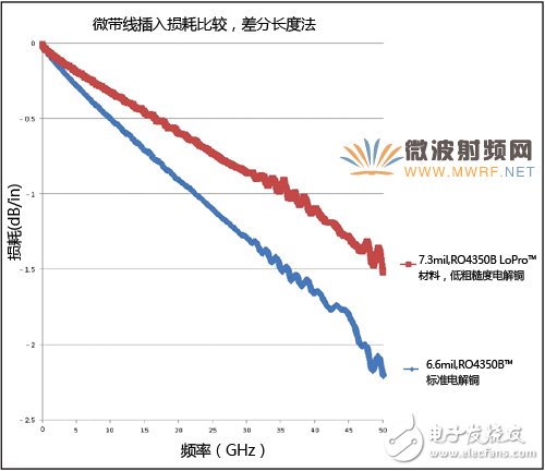
Figure 3. Circuit loss comparison using different roughness copper foils on the same material
To further compare the effects of copper foil roughness, Figure 3 shows the circuit insertion loss comparison using different types of copper foil on the same material. The Rogers standard RO4350BTM laminate copper foil used has an average roughness of 2.5 um RMS, while the RO4350 BLoProTM laminate copper foil has an average roughness of 0.6 um RMS. Although the curve results at 50 GHz have some noise jitter, the trend is obvious, and the smoother the copper surface corresponds to the lower the insertion loss. Of course, there are subtle differences (0.7 mils) in the media thickness of the two materials, but for thinner materials, conductor losses will account for the majority of the total loss.
The final surface treatment of the circuit also affects the conductor loss of the circuit, especially in the high frequency band. In general, many of the metals used in PCB surface treatments are less conductive than copper, and additional surface treatments result in increased conductor losses. For example, the most commonly used chemical nickel gold (ENIG) surface treatment in PCBs, because of the poor conductivity of nickel than copper, the use of ENIG surface treatment will inevitably lead to an increase in conductor loss. A typical ENIG surface treated metal conductor stack begins with a base copper of the material, deposits nickel over the copper to prevent oxidation of the copper, and finally deposits gold over the nickel. From the thickness point of view, the growth of gold is a self-limiting process and the thickness is generally about 0.2 um, while the thickness of nickel is generally about 5 um. Taking into account the skin depth of the millimeter wave band, the current will completely cover the nickel layer and part of the gold layer. As the frequency increases, the gold plating layer is completely covered. However, since the conductivity of gold is still worse than that of copper, the use of ENIG surface treatment will eventually lead to an increase in circuit conductor loss.
Figure 4 shows the effect of using bare copper on the same circuit substrate and using ENIG for circuit insertion loss. The results of Figure 4 explain a number of issues. Circuit insertion loss using ENIG surface treatment is higher than bare copper structure circuits. However, in the low frequency band, the insertion loss characteristics of the two circuits are different. This is mainly because the nickel layer is thicker, and the low-band current is mostly distributed in the nickel metal due to the skin depth, but is rarely distributed in the copper and gold. When the frequency rises to 20 GHz, the current begins to distribute in gold due to the skin depth effect. As the frequency increases further, more gold is used and the insertion loss curve of the ENIG circuit becomes parallel to the loss curve of the bare copper structure.
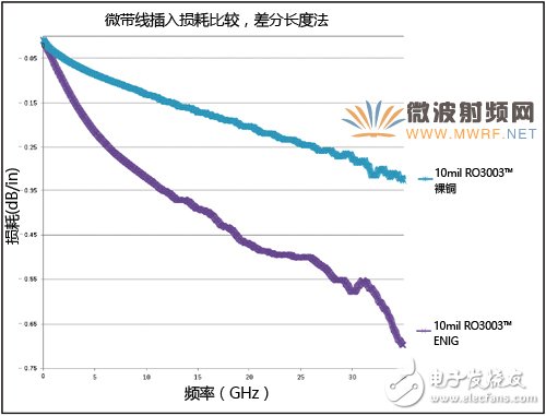
Figure 4. Comparison of insertion loss between bare copper structures and ENIG surface treated microstrip transmission lines using the same material
silverThe conductivity of sterling silver is higher than that of pure copper. In the surface treatment process of PCB, the use of the sinking silver process is actually a silver alloy instead of pure silver. The alloy is approximately pure silver and is approximately conductive in copper. The silver-silver process is self-limiting, and the added silver is also a thin layer with a thickness of 0.2 um. Compared with gold, silver is gradually oxidized and gold does not. Although the oxidation of silver causes a change in the color of the surface, this oxidation has little effect on the insertion loss of the circuit. The authors of this paper have shown that oxidation does not affect the insertion loss of the circuit in the study of circuits that have been oxidized for 2.5 years. It is worth mentioning the problem of signal transition in the test of Figure 4. The curve data in Figure 4 was obtained with a commercial vector network analyzer with a 50 GHz frequency cap. However, due to the signal transition problem, there is noise above 35 GHz, so the data in the figure only measures 35 GHz. If a more efficient signal transition is used, the ENIG insertion loss curve and the bare copper insertion loss curve in Figure 4 should converge parallel in the 25 GHz to 50 GHz or higher frequency range.
As mentioned earlier, insertion loss has many components, and understanding these components is very helpful for designers of millimeter wave circuits. The MWI application developed by Rogers can simulate the various components of insertion loss, which can be downloaded from the Rogers homepage (). The program is based on the description of impedance and loss characteristics of microstrip transmission lines proposed by Hammerstad and Jenson. MWI software can also predict the radiation loss of the microstrip line. The calculation is based on Wadell's research results, which show that the software predictions have high accuracy.
Figure 5 shows the insertion loss and composition of two different thickness circuits obtained using MWI-2010 simulation. In the circuit simulation model, the width of the wire ensures that the transmission line impedance is 50Ω, the Dk of the material used is 3.66, and the copper thickness is 1 oz. If the radiation loss is neglected, the contrast between dielectric loss and conductor loss is very obvious. When the frequency is below 15 GHz, in a thin 10 mils circuit, the conductor loss is a major component of the total insertion loss. The dielectric loss in a thick 30 mils circuit is higher than the conductor loss. In this frequency range, the circuit designer needs to consider the thickness of the board when selecting the material with a certain copper foil (conductor loss) and loss factor (medium loss). In the frequency range shown in Figure 5, for a 30 mils circuit, the radiation loss at 15 GHz is very significant, but it is not the main part of the insertion loss.
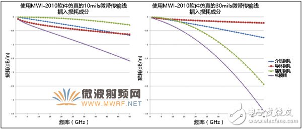
Figure 5. Microstrip transmission line insertion loss (total loss) and composition comparison of different thicknesses of the same circuit material
Radiation lossFigure 5 shows that the radiation loss depends on the operating frequency and the thickness of the circuit. At frequencies below 15 GHz, the radiation loss of a 10 mils circuit is not significantly negligible, while the radiation loss of a 30 mils circuit is significant. Therefore, in general, the use of a thin circuit substrate thickness can reduce the radiation loss. When the frequency rises to the millimeter wave band (greater than 30 GHz), the radiated loss of a thick circuit is a major part of the total loss compared to a thin circuit.
Radiation loss is related to the thickness of the PCB material and to the Dk value of the PCB material. The higher the Dk value of the circuit material, the lower the radiation loss of the circuit, but this will result in higher conductor losses in the circuit. In addition, the larger the Dk value of the circuit material, the narrower the width of the signal conductor when the same impedance value is achieved. The narrower the signal conductor, the higher the conductor loss will be.
The design of the circuit also affects the radiation loss because any impedance mismatch is usually accompanied by a certain amount of energy radiation. Impedance mismatch in RF/microwave circuits is very common, which is closely related to the specific design of the circuit. For example, stripline circuits typically have no radiation loss, while the microstrip line circuit of Figure 5 is susceptible to radiation loss, the extent of which is related to circuit thickness and other factors. When the radiation loss becomes a design problem, the GCPW circuit can effectively reduce the radiation loss. This conclusion is elaborated in the study of 50 GHz GCPW circuits and other circuit optimization signal transitions.
In the millimeter wave high frequency band, a good transition of the signal interface is an important factor to ensure circuit performance. Signal transitions and radiated losses are related because effective signal transitions enable efficient transition of signal energy from one transmission mode to another, which reduces radiation loss. For example, a typical RF connector operates in a transverse mode (TE) and a planar PCB operates in a transverse electromagnetic (TEM) mode. The working mode of the GCPW and the microstrip line is the quasi-TEM mode, and the working mode of the strip line is the standard TEM mode. When the transmission mode changes, such as the connection of the connector to the board, any parasitic reactance or impedance mismatch will cause the circuit to generate radiation loss.
Designers of millimeter-wave high-frequency circuits should often contact suppliers of high-frequency materials to better understand the comprehensive performance of different high-frequency circuit materials and different PCB materials for millimeter-wave circuits. Many circuit substrates can be combined with different types and different roughnesses of copper for use. In a single product line, there are many different circuit materials available from the perspective of Dk and loss factor. High-frequency circuit material suppliers are happy to work closely with circuit designers to optimize the performance of existing and new microwave/millimeter wave circuits.
Heating Mouse Pad,Heated Computer Mouse Pad,Heated Mouse Pad,Usb Heated Mouse Pad,Hand Warmer Mouse Pad
Ningbo Sinco Industrial & Trading Co., Ltd. , https://www.newsinco.com