
Abstract: In the past two years, the development of compound semiconductors has received strong support from the state. Compound semiconductors have high electron mobility, high reverse breakdown voltage and other characteristics and have been widely used in mobile terminals. The creation of a compound semiconductor device model for use by integrated circuit designers to design complex integrated circuits is one of the key technologies for integrated circuit foundries. Compound heterogeneous PN junction is the most basic structure of HBT. It is necessary to systematically analyze and create a circuit simulation model of PN junction. After decades of development, the mathematical model of the PN junction based on the Si process has been perfected, but there is a lack of related works on the heterogeneous PN junction model of compound semiconductors. The mathematical model based on Si process is applied to the GaAs process and the circuit simulation model is created using Verilog-A. Finally, the extraction method of the corresponding model parameters is given to ensure that the simulation results of the model DC characteristics and RF characteristics are highly consistent with the actual test data. By measuring and modeling the PN junction of the gallium arsenide process, the accuracy and versatility of the Verilog-A model can be obtained.
introduction
In recent years, China has vigorously developed the manufacturing technology of compound semiconductors. Compared with BJT and CMOS using Si process, HBT pHEMT manufactured by GaAs process is widely used to design PA and LNA for mobile terminals because of its high electron mobility and high breakdown voltage.
The PN junction is the most basic structure of a semiconductor device and is a basic unit of a semiconductor device such as a transistor and a field effect transistor. Therefore, it is particularly important to measure and model the electrical properties of heterojunction PN junctions of compound semiconductors.
This article discusses the entire process of modeling a semiconductor device from the physical structure of the PN diode, measurement of the electrical characteristics, optimization of the device model and its parameters, and finally the comparison of the model.
The mathematical model of the device, scientists have done a lot of research, but also continue to upgrade the device model, so that the device model and the upgrading of semiconductor technology to match. Different semiconductor processes, such as Si, GaAs, GaN, etc., the PN junction model is only the difference in model parameters. Therefore, in the extraction of model parameters, it is common practice to use modeling software to adjust the parameters so that the simulation curve and the measurement curve coincide. Taking into account the relative simplicity of the mathematical model of the diode, this article will use the conventional method of modeling to extract parameters, by the way briefly introduces the mathematical analysis of the extraction means.
Finally, it is the realization of the device's mathematical model to the circuit simulation model. This paper uses Verilog-A language to describe the syntax. And summarize the general steps that need to be experienced in the diode modeling process.
1, PN junction electrical performance measurement
1.1 DC Characteristics
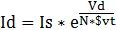
Using a semiconductor analyzer, the forward and reverse DC characteristics of the PN junction were measured.
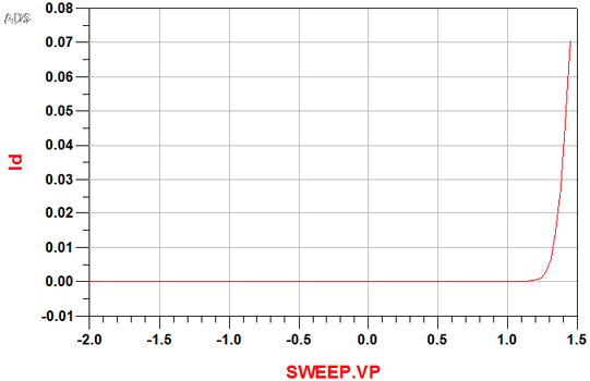
Figure 1, the DC IV curve of the diode
1.2 RF Characteristics
The CV curve was tested using a high frequency measurement environment consisting of a semiconductor analyzer and a vector network analyzer.
Vector network analyzer set fixed frequency 110MHz, semiconductor analyzer sweep bias -2 ~ 1.45V; get a set of S_vs_V data, converted to Y_vs_V, and then through a mathematical transformation: Zd = -2 / (Y12 + Y21), get Zd_vs_V impedance - Bias curve, as follows:
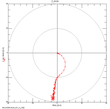
Figure 2. Zd_vs_V/impedance-bias curve for diodes
From figure (2) we can conclude that the real part of Zd has a negative value and is equivalent to a negative resistance. This indicates that the quantum tunneling effect occurs in the barrier region when the PN junction is reverse biased [1]. The electrons will cross the barrier to form a negative resistance.
In the junction capacitance extraction, since the frequency of the vector network analyzer is 110 MHz, the imaginary part of Zd is approximately a pure capacitor, so there is: imag(Zd)=-1/(2*PI*freq*C), which can be obtained through conversion. The C_vs_V curve is plotted as follows:
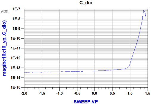
Figure 3, CV curve of the diode, logarithmic coordinates
2, mathematical model
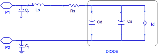
Figure 4. Small signal equivalent circuit
Among them, DIODE is an internal diode (Intrinsic diode); the junction capacitance of the diode is composed of Cs and Cd. Ls and Rs are the parasitic inductance and parasitic resistance of the lead. In addition, according to the test structure of the DUT, the diode also has a set of capacitances Cp to ground. The above conversion process knows that the measured RF CV curve is obtained by converting Y12 and Y21 of the pi-type network. This pair of capacitors Cp The CV curve has no effect.
2.1 DC mathematical model [2]
Id=:
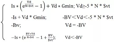
among them:
Is: saturation current (leakage current); N: emission coefficient (1≤N≤2); BV: Breakdown voltage; $vt=K*T/q; Ibv=Is*BV/$vt;
2.2 RF mathematical model [2]
The model of the junction capacitance is described by the power Q.
When Vd<Fc*Vj:
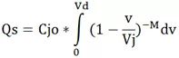
When Vd≥Fc*Vj:
among them:
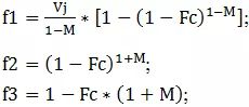
Vj: Junction potentialM: Grading coefFc: Forward bias junct parmFcp = Fc * Vj;
3, model parameter extraction
DC parameter extraction
Near the diode turn-on voltage, the IV curve represented by the logarithmic scale is linear. In this linear region, the contribution of Id's last two terms Is and Vd*Gmin to Id is neglected, as shown in Fig. (4); therefore, the DC model can be approximated for:
Take the natural logarithm on both sides, there are:
Ln(Id)=ln(Is)+Vd/(N*$vt)
A new curve is obtained, from which the slope of the linear region can be extracted to N, and the linear region is extended to the axis of Vd=0, and Is can be extracted.
Then, in the high current area, do the extraction of Rs.
The modeling approach is to adjust the model parameter values ​​so that the model curve and the measurement curve overlap. Pictured:
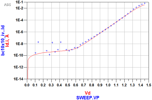
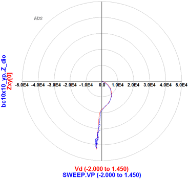
Figure 5, parameter extraction
4, circuit simulation model creation
Verilog-A mainly describes the relationship between the voltage and current of the nodes and branches that make up the circuit network. In the equivalent circuit model of Fig. (4), it is necessary to implement Verilog-A description. In addition to the essential diodes, it is necessary to solve the resistance, inductance, and capacitance components. Resistive element: V=R*I; inductive element: V=L*ddt(I); capacitive element: I=C*ddt(V). The first two are the equivalent components of parasitic parameters and are ideal components. However, the node capacitance C of the diode is no longer a constant, but a function of the bias voltage Vd. Therefore, it is expressed by the power Q, ie, I=ddt(Q).
And there are:
Q=Qs+Qd;
among them:
Qd is determined by the transit time parameter: Qd = Tt * Id. From the point of view of the impedance characteristics of the PN junction, the transit time parameter Tt contributes a negative resistance, which is caused by the electron quantum tunneling effect when the PN junction is reversed biased [1].
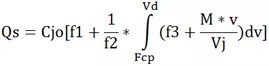
When Vd<Fc*Vj:
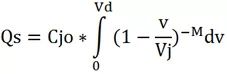
On the formula, order 
Then, v=Vj*(1-u), there is  , =>
, =>
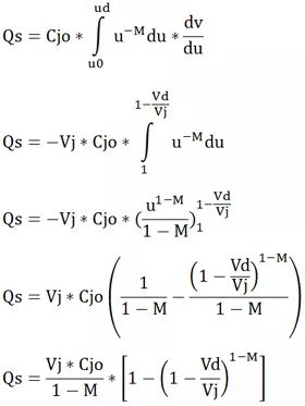
When Vd≥Fc*Vj:
Integral part of the above formula, order 
then,  ,Have
,Have  ,
,
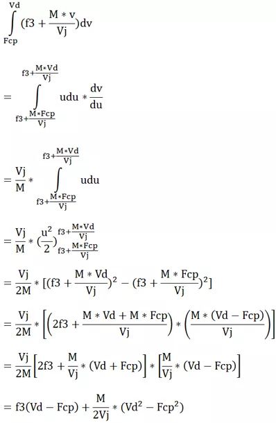
which is:

According to the above formula, the diode's Verilog-A model is described as follows:
`include "disciplines.vams"`include "constants.vams" module PN_DIODE(anode, cathode); inout anode, cathode; electrical anode, cathode; parameter real Area = 2; //Area scaling factor parameter real Is = 1.2e- 15; //Saturation current [A] parameter real Rs = 0.66; //Series resistance [Ohm] parameter real Ls = 170e-12; // Series inductance[H] parameter real N = 1.80; //Ideality parameter real Tt = 1.2e-10; //Transit time [s] parameter real Cjo = 2.3e-14; //Junction capacitance [F] parameter real Vj = 1.06; //Junction potential [v] parameter real M = 0.336; //Grading Coef parameter real Fc = 0.99; //Forward bias junct parm parameter real BV = 25.45; //Breakdown Voltage parameter real Gmin = 1.4e-9; //minimum distance conductance real Vd, Id, Qd, Ibv; real f1, f2 , f3, Fcp; electrical in1, in2; analog begin f1 = (Vj/(1 - M))*(1 - Pow((1 - Fc), (1 - M))); f2 = pow((1 - Fc), (1 + M)); f3 = 1 - Fc * (1 + M); Fcp = Fc * Vj ; Ibv = Is * BV / $vt; Vd = V(in1, cathode); Id = I(in1, cathode); // Intrinsic diode if (Vd < -5 * N * $vt) begin if (Vd == -BV) I(in1, cathode) <+ -Area * Ibv; else if (Vd > -BV) I(in1, cathode) <+ -Area * Is +Vd * Gmin; else I(in1, cathode) <+ -Area * Is * (exp( -(Vd + BV) / $vt) - 1 + BV / $vt); end else I(in1, cathode) <+ Area * Is * (exp(Vd / (N * $ Vt)) - 1) + Vd * Gmin; // Capacitance (junction and diffusion) if (Vd <= Fcp) Qd = Tt * Id + Area * Cjo * Vj * (1 - pow ((1 - Vd / Vj) , (1 - M)))/(1 - M); else Qd = Tt * Id + Area * Cjo * (f1 + (1 / f2) * (f3 * (Vd - Fcp) + (0.5* M / Vj) * (Vd + Fcp) * (Vd - Fcp))); I(in1, cathode) <+ ddt (Qd); V(in2, in1) <+ I(in2, in1) * Rs; V(anode, in2) <+ Ls * ddt(I(anode,in2)); endendmodule
5, summary
This article discusses the small-signal model of a diode, which is suitable for PN junctions composed of semiconductor materials and Schottky PN junctions composed of metal semiconductors. In addition, the model parameters of the discussed diodes apply to the heterojunction composed of Base and Collector materials for the GaAs HBT process.
A Solar Panel, or photo-voltaic (PV) module, is an assembly of photo-voltaic cells mounted in a framework for installation. Solar panels use sunlight as a source of energy to generate direct current electricity.
The main two types of solar panels. Each of these types of solar cells is made in a unique way and has a different aesthetic appearance.
- Mono crystalline
- Poly crystalline

Polycrystalline Solar Cells,Solar Mono Panel,Poly Solar Cell,Mono Or Poly Solar Panels
NANTONG RONGCHANG IMPORT&EXPORT CO.,LTD , https://www.ergsolarcn.com