
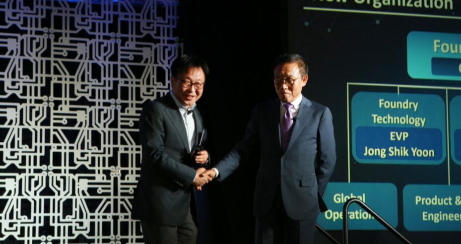
ã€Global Network Technology Reporter Chen Jian】 May 25 news, in the early hours of today, Samsung held a press conference, the conference announced a long-term circuit plan, to launch 4nm process in 2020 .
As a rare Samsung device that covers almost every aspect of the entire industrial chain of the technology circle, Samsung Samsung Semiconductor has developed rapidly in the past two years. The Samsung S8 has already used its own 10nm process chip. The entire mobile electronics industry is affected by Samsung's supply chain.
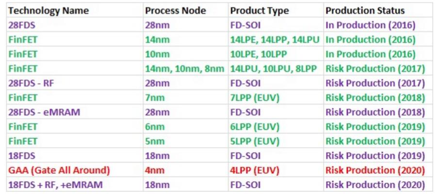
Samsung plans to plan the next three years to 2020, Samsung will advance nano-technology step by step. In 2017, we will try out the 8nm process this year. We will advance to the 7nm process in 2018, 6nm in 2019, and 5nm in the second half until we try to produce 4nm in 2020.
Samsung said it will adopt a new production process in 2018, a new technology called EUV lithography. This technology will use a brand new circuit board printing. Samsung said that if this technology is adopted, production steps, cost, and chip performance can be greatly reduced. Samsung also said that the lithography machines used in its fabs can already reach 1,000 wafers per day. In the future, Samsung hopes to increase production by 50% to 1,500 wafers. At the same time, Samsung also announced that it will introduce the most advanced EUV lithography machine into wafer manufacturing in 2018.
Previously, there was news that Samsung is still aggressively promoting the chip foundry business. At present, the top chips including the Snapdragon 835 mobile platform are manufactured by Samsung. Samsung plans to spin off the chip manufacturing business to form a new department. Positive and TSMC Start the competition. Don't know if Intel that squeezes toothpaste can give some strength!
Barium titanate lead-free piezoelectric ceramics are important basic materials for the development of modern science and technology, which was widely used in the manufacture of ultrasonic transducers, underwater acoustic transducers, electroacoustic transducers, ceramic filters, ceramic transformers, ceramic frequency discriminators, high voltage generators, infrared detectors, surface acoustic wave devices, electro-optic devices, ignition and detonation devices, and piezoelectric gyroscope and so on.
Application: military, ocean, fishery, scientific research, mine detection, daily life and other fields.

Piezoelectric Ring,Lead Free Piezoelectric Ring,Piezo Electric Ring,Lead Free Piezo Rings
Zibo Yuhai Electronic Ceramic Co., Ltd. , https://www.yhpiezo.com