
Throughout a high-speed printed circuit board (PCB), through-holes have been criticized for reducing signal integrity performance. However, the use of vias is unavoidable. On a standard board, the components are placed on the top layer and the differential pairs are routed on the inner layer. The electromagnetic radiation of the inner layer and the crosstalk between the pair and the pair are lower. A via must be used to connect the components on the board plane to the inner layer.
Fortunately, a transparent via can be designed to minimize the impact on performance. In this blog, I will discuss the following:
Basic components of vias
Electrical properties of vias
A method of constructing transparent vias
Test results of differential via structure
1. Basic knowledge of via structure
Let's start by examining the components of the simple via that connect the top transfer line to the inner layer. Figure 1 is a 3D diagram showing the structure of a via. There are four basic components: signal vias, via stubs, via pads, and isolation pads.
A via is a metal cylinder that is plated outside the via between the top and bottom layers of the board. Signal vias connect the transmission lines on different layers. The via stub is the unused portion of the via. Via pads are ring-shaped pads that connect vias to the top or internal transmission lines. The isolation disk is an annular gap in each power or ground plane to prevent short circuits to the power and ground planes.
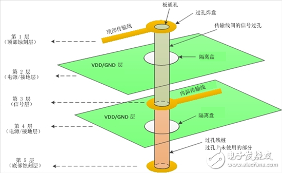
Figure 1: 3D diagram of a single via
2. Electrical properties of via components
As shown in Table 1, let's take a closer look at the electrical properties of each via component.
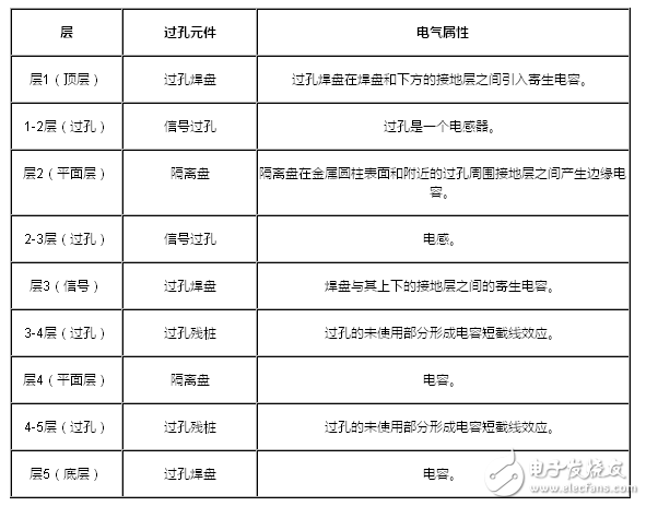
Table 1: Electrical properties of the via components shown in Figure 1.
A simple via is a series of π-type networks consisting of capacitor-inductor-capacitor (CLC) components in two adjacent layers. Table 2 shows the effect of the via size.
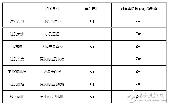
Table 2: Visual effects of via size
By balancing the inductance and parasitic capacitance, it is possible to design vias with the same characteristic impedance as the transmission line, so that it does not have a particular effect on board operation. There is no simple formula to convert between via size and C and L components. The 3D electromagnetic (EM) field solver can predict the structural impedance based on the dimensions used in the PCB layout. By repeatedly adjusting the size of the structure and running 3D simulations, the via size can be optimized to achieve the required impedance and bandwidth requirements.
3. Design a transparent differential via
As we discussed in the previous post, line A and line B must be highly symmetrical when implementing differential pairs. These pairs are routed within the same layer. If a via is required, the holes must be drilled in close proximity to the two lines. Since the two vias of the differential pair are close together, an elliptical spacer disk shared by the two vias can reduce parasitic capacitance instead of using two separate isolation disks. Ground vias are also placed next to each via so that they provide a ground return path for the A and B vias.
Figure 2 shows an example of a ground-signal-signal-ground (GSSG) differential via structure. The distance between two adjacent vias is called the via pitch. The smaller the via pitch, the more mutual coupling capacitors.
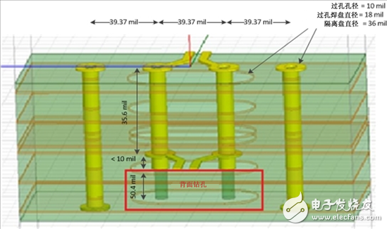
Figure 2: GSSG Differential Via Using Back Drill
Don't forget that via stubs can seriously affect high-speed signal integrity at transmission rates above 10Gbps. Fortunately, there is a back-drilled PCB fabrication process that can drill holes in unused via cylinders. Depending on manufacturing process tolerances, the backside drill removes unused via metal and minimizes via stubs to less than 10 mils.
The 3D EM simulator is used to design differential vias based on the required impedance and bandwidth. This is an iterative process. This process repeatedly adjusts the via size and runs the EM simulation until the desired impedance and bandwidth are achieved.
UV Photocatalytic Exhaust Gas Purifier
Uv Photolysis Device,Gas Purification System,Waste Treatment Equipment,Uv Photocatalytic Exhaust Gas Purifier
Dongguan V1 Environmental Technology Co., Ltd. , https://www.v1airpurifier.com