
Using different voltages on the same chip has always been a real problem.
Whether you want to mix high-voltage analog signals with low-voltage storage or want to use multiple VDDs on the same digital chip, you need to address the effects of different voltages on the wiring and circuit layout. In addition, whether you are more concerned with signal integration or more concerned with long-term stability, you have to face the most basic problem: How far do these voltage areas need to be at least if there is no problem?
In the past, the best way to solve this problem was to mark the top layer of the PCB so that people know the voltage used in that area. Design and validation also use the markup layer in their operations, which seems to be pretty good.
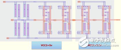

Use a marker layer to distinguish between different voltage regions
This method is not bad for designs with few different voltage regions and the difference between each voltage is obvious. Using this method requires the designer to clearly understand the extent of each area and use the appropriate marking layer... and also ensure that the designer has enough time to do this and will not forget.
Of course, the world of IC design won't be that simple forever. You will encounter more and more voltages, more and more different power domains. In addition, many designs are now size sensitive. In order to save working area, sometimes high voltage lines have to be routed through the low voltage area. These factors require more precise precision and control, which requires a polygon-level voltage-dependent DRC (design rule check) check method. The idea of ​​this method is very simple. Unlike the use of the markup layer mark, it is only necessary to simply put the voltage information into the polygon area, and the verification tool can calculate the closest space wiring rule according to the range of the maximum/minimum voltage.
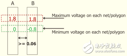
A simple demonstration of the polygon-level voltage-dependent DRC (design rule check) check method
When using this method, the DRC tool can use the actual maximum/minimum voltage information to determine what minimum spacing rule to apply. For example, if the maximum possible voltage difference between two adjacent traces is 1.5V, then the X rule is used. If this value is 2.1V, another rule Y is used. By this inspection method, the area required for the circuit can be minimized, and manufacturing process limitations are ensured.
The most obvious challenge with this approach is that the maximum and minimum voltage values ​​must be confirmed and annotated into the layout network. Once the voltage is generated, it needs to be marked into the layout. But layout engineers don't want to waste time on entering such information. Is there any way to do it automatically?
The method of generating the maximum/minimum voltage depends on the design flow. For the analog design, the SPICE simulation is complete and covers the entire dynamic range of each node, so each region can be directly derived from the existing simulation stream. Maximum/minimum voltage value. For digital design, the difficulty is much greater.
For digital design, we recommend using automated tools to transfer voltage from the pin to the internal network. These tools should be able to pass the voltage of each pin to the internal node and then provide a complete dynamic range for each internal network. The tool then automatically marks the maximum/minimum voltage on each layout and signs the DRC.

Voltage-dependent DRC process for sign-off and interactive repair. The combination of Calibre PERC and Calibre nmDRC gives you a complete process to generate the required voltage information on the layout used and validate against the factory's DRC sign-off requirements.
Errors from this process are highlighted in the design environment, as are other validation errors. However, the result will only contain the information of the error itself (voltage difference and related errors); in order to eliminate this error, the layout engineer needs to know more about this error. For example, if there is an error involving two regions, the voltage difference between the two is 2.2V, then the interval should be X... But where do these voltage differences come from? What voltage value does that area have? This information appears in the verification process and does not appear in the design environment or results.
Fortunately, you can export voltage and routing network information in a format and import it into the OpenAccess database as a series of restrictions. You should use a tool that recognizes this information and provide it to the user interaction, and add this voltage information to the polygon for cross-certification.
By combining the right automation tools with a custom design environment, you can provide a complete system that implements, optimizes, and validates voltage-dependent layouts for smaller, more efficient layouts and ultimately for multi-voltage domain projects. Save time and money.
Lifepo4 Cells,Li-Ion Battery,Deep Cycle Lifepo4 Battery,Rechargeable Lifepo4 Battery
Zhejiang Xinghai Energy Technology Co.,Ltd , https://www.headwayli-battery.com