
Ultra-wide input range industrial control power supply design
When designing the auxiliary power supply for industrial control, the third generation miniature switching power supply of TInySwitch-Ⅲ series launched by American PI Corporation can be used. At present, the universal AC input voltage range is u = 85 ~ 265V. However, when 18V <u <75V, the chip cannot provide enough bias to maintain normal operation, which greatly limits the application of TInySwitch-Ⅲ series products in the low-voltage field. In order to solve the above-mentioned problems and enable TInySwitch-Ⅲ to work normally under ultra-low AC input voltage, it is necessary to design a suspended high-voltage constant current source from the outside.
Performance characteristics of TInySwitch-â…¢ series products
TinySwitch-Ⅲ series products include TNY274P ~ TNY280P, TNY274G ~ TNY280G and other 14 types. This series of products mainly has the following characteristics:
◠The maximum output power of TinySwitch-Ⅲ series products is 36.5W (TNY280P / G type). By selecting the capacitance of the BP / M terminal, the internal leakage limit flow point can be set from the outside. In addition to TNY274P / G, each model has 3 different limit current values ​​for users to choose. The advantage is that when replacing with adjacent models, there is no need to redesign the high-frequency transformer, and there is no need to change the peripheral components.
â— Users can optimize power supply design from the perspective of maximizing power supply efficiency and obtaining maximum output power. Choose a higher leakage limit current point for higher peak power or higher continuous output power in open power modules; and a lower limit current value can improve the efficiency of the sealed power adapter / battery charger .
â— The efficiency of the traditional pulse width modulation (PWM) switching power supply decreases significantly as the load decreases. TinySwitch-â…¢ adopts the on / off control method, which can meet the requirements of the standby power supply and the no-load power consumption energy saving standard. The no-load power consumption is less than 150mW; after adding the bias winding, it can be reduced to less than 50mW.
â— With input under-voltage protection, output over-voltage protection and power switch tube adaptive on-time extension function.
Working principle of TinySwitch-â…¢ series miniature switching power supply
The internal block diagram of TinySwitch-Ⅲ is shown in Figure 1, where S and D are the source and drain of the internal power MOSFET (the four sources are connected internally). EN / UV is the "enable / undervoltage" dual-function lead-out terminal. Under normal circumstances, the power MOSFET can be turned on and off through this terminal; if an external resistor is connected between this terminal and the DC input voltage Check if the input is under voltage. BP / M is a bypass / multi-function terminal. When it is simply used as a bypass terminal, a bypass capacitor of 0.1μF is connected between this terminal and ground (S pole). The BP / M terminal also has the characteristics of a multi-function terminal: first, the capacity of the leakage limit can be set by changing the capacity of the bypass capacitor; second, the terminal can also provide a shutdown function, the specific method is at the output terminal of the feedback voltage and A voltage regulator tube is connected between the BP / M terminals to realize output overvoltage protection.
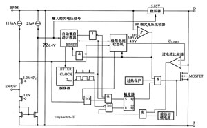
Figure 1 Internal block diagram of TinySwitch-â…¢
TinySwitch-â…¢ integrates a power MOSFET with a withstand voltage of 700V and an on / off controller. Unlike traditional PWM controllers, it uses a simple on / off controller to regulate the output voltage. It mainly includes an oscillator, a 5.85V voltage regulator, a 6.4V voltage regulator for bypass clamp, enable detection and logic circuit, limit current state machine, under voltage, over current and over temperature protection circuit and automatic restart counter.
The corresponding relationship between the limit current ILIMIT of TinySwitch-Ⅲ and the bypass capacitor CBP is shown in Table 1. Taking TNY279P / G as an example, when the bypass capacitor CBP = 0.1 μF, select the standard limit current ILIMIT = 650 mA (typical value, the same below); when the bypass capacitor CBP = 1 μF, select the lower limit current ILIMIT- = 550mA; when the bypass capacitor CBP = 10μF, select a higher limit current ILIMIT + = 750mA, the difference between the three is 100mA in turn. The biggest advantage of this design is to ensure good compatibility between adjacent models. For example, INYMIT- = 550mA of TNY279P / G, which happens to be the limit current value of the adjacent model TNY278P / G; and ILIMIT + = 750mA of TNY279P / G, which is the limit current value of the adjacent model TNY280P / G, the rest analogy.

The circuit design of the industrial control power supply with ultra wide input range is composed of TinySwitch-Ⅲ series products TNY280P. The circuit of the industrial control power supply with 3W ultra wide input range is shown in Figure 2. The remarkable feature of this power supply is the extremely wide AC voltage input range (18 ~ 265V), the output voltage is + 5V, and the output current is 600mA. The power supply efficiency can reach 65%, and the no-load power consumption is less than 200mW when the AC input voltage is 230V. Application areas for this power supply include auxiliary power supplies for industrial control.

Figure 2 The circuit of 3W ultra wide input range industrial control power supply formed by TNY280P
The minimum drain voltage of TinySwitch-â…¢ series products can start and work normally is 50V. Normally, when the AC input voltage u> 85V, the chip can provide self-supplied bias. However, when 18V <u <75V, the chip cannot provide enough bias to maintain normal operation, which greatly limits the application of TinySwitch-â…¢ series products under low voltage. In order to solve the above problems and enable TinySwitch-â…¢ to work normally under ultra-low AC input voltage, a floating high-voltage current source needs to be added from outside of TNY280P to continue supplying the bypass terminal BP / M at low voltage. The circuit of the floating current source is shown in Figure 3. It includes 7.5V regulator VDZ1 (1N5236B), PNP transistor VT1 (ZTX558), NPN transistor VT2 (ZTX458), diodes VD2 and VD4, resistors R4 ~ R6. Among them, VD2 is a half-wave rectifier; VD4 is an isolation diode, which can isolate the current source from other circuits.
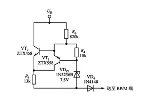
Figure 3 Circuit of floating current source
Both ZTX558 and ZTX458 are high-reverse-voltage transistors produced by Zetex Semiconductors in the UK. Among them, ZTX558 belongs to the PNP type high back pressure transistor, the main parameters are the collector-emitter reverse breakdown voltage U (BR) CEO = -400V when the base is open, and the collector-base of the emitter is open Reverse breakdown voltage (that is, collector junction reverse breakdown voltage) U (BR) CBO = -400V, maximum collector current ICM = -200mA, common emitter current amplification factor hFE ≤ 300, maximum power consumption PCM = 1W. ZTX458 belongs to NPN type high back pressure transistor, the main parameters are U (BR) CEO = 400V, U (BR) CBO = 400V, maximum collector current ICM = 300mA, hFE≤300, PCM = 1W.
After the AC voltage of 18-265V undergoes VD2 half-wave rectification, a bias voltage UB of pulsating DC is obtained, which is added to the input end of the floating current source. This current source can provide a constant current of approximately 600μA to the BP / M terminal of the TNY280P over the entire input voltage range. First assume that this circuit only uses the transistor VT2, it can be considered that the voltage regulator tube VDZ1 provides a reference potential UB2 to the base of VT2. Since the sum of the launch junction voltage (UBE2) of VT2 and the voltage drop (UR5) on R5 is equal to the stable voltage value UZ of the regulator tube, and UBE2 is approximately a constant voltage when the ambient temperature is constant, so UR5 is also a fixed Voltage, use R5 to set the constant current value. However, in fact, the range of the AC input voltage is wide, and the range of the bias current provided by the regulator tube is very large, which will cause the set constant current value to shift. To overcome the above problems, a constant bias current needs to be provided by PNP transistors VT1 and R4. Let the launch junction voltage of VT1 be UBE1, and the constant bias current IB1 = UBE1 / R4 set by R4. Obviously, IB1 is not affected by input voltage changes.
The relationship between the bias voltage (UB) and the total bias current (IB) is shown in Figure 4. It can be seen from the figure that VT2 provides a constant bias current IB2 at a lower input voltage, and VT1 provides a constant bias current IB1 at a higher input voltage. It can be divided into the following three situations:
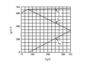
Figure 4 The relationship between bias voltage and total bias current
1 When the bias voltage UB≈50V (that is, the rectified and filtered DC input voltage UI≈50V), VT2 provides a constant bias current IB2 to the TNY280P, and the total bias current IB = IB2.
2 When the bias voltage UB> 50V, the current flowing through VT2 will decrease linearly, while the current flowing through VT1 increases linearly. At this time, VT1 and VT2 jointly provide a constant bias current to TNY280P. Set the current IB = IB1 + IB2, where IB2> IB1.
3 When the bias voltage reaches the maximum value (UB = 375V), the constant bias current is mainly provided by VT1, IB = IB1 + IB2, but among them IB1> IB2.
The total bias current provided by this circuit IB≈600μA.
The AC input voltage of 18 ~ 265V passes through the half-wave rectifier filter circuit composed of VD1, C1 and C2 to obtain the DC input voltage UI, which provides high-voltage DC for the flyback switching power supply. C1 and C2 also form a π-shaped filter with the inductor L, which is used to reduce the series mode electromagnetic interference. Y capacitor C7 is used between the primary and secondary windings of the high-frequency transformer to filter out common mode interference. The primary side clamping circuit is composed of VD3 (1N4007GP), R1, R2 and C3. Rectifier VD5 adopts BYV27-200 type 2A / 200V ultra-fast recovery diode, and its reverse recovery time trr <25ns. The output voltage is set by the sum of the voltage drops of the voltage regulator VDZ2 and the photocoupler PC817A. VDZ2 uses a 4.3V voltage regulator 1N5229B, the forward voltage drop of the LED is approximately 1V, and the set no-load output voltage is 5.3V.
TNY280P adopts on / off control method, it receives the feedback voltage of the secondary winding through the optocoupler, and then enables or disables the on / off of the internal MOSFET to keep the output voltage stable. Once the current flowing from the EN / UV terminal exceeds the turn-off threshold current (115μA), the switching cycle will be skipped; when the current flowing from the EN / UV terminal is less than the turn-off threshold current, the switching cycle will be re-enabled.
Design Points
1 The high-frequency transformer adopts EF20 type ferrite core, and the primary winding is wound with 32 turns of Φ0.33mm enameled wire. The secondary winding is wound with 8 turns of Φ0.40mm enameled wire. The inductance of the primary winding LP = 278μH (with an error of ± 12% allowed), and the maximum leakage inductance LP0 = 12μH. The lowest resonant frequency of the primary winding is 1MHz.
2 Because the input voltage range of this power supply is very wide, the inductance LP of the primary winding must be small enough (practically choose 278μH) in order to make the TNY280P work at the edge of continuous mode. However, when LP is small, the current rise rate di / dt will increase. If necessary, the chip with larger output power in the TinySwitch-Ⅲ series can be used.
3 The resistance value of R1 in the clamp circuit should not be too small, otherwise it will increase the no-load power consumption.
LED DJ Display
LED DJ Booth is used different product models and structures as different conditions, which can be customized to the scene modeling. It can be spliced out the unique shape with different sizes of triangles, rectangles, hexagon. Unique DJ Table is not limited to kinds of environment. The application of the relevance and the shape of DJ LED Video Wall can enhance scene recognition.
LED Bar Display will not only present a delicate and realistic color performance through the synchronization adjustment, but also is compatible with different sources of input such as TVV, HDV, DVI, VGA, SDI. We adopt SMD technology to achieve super-wide viewing angle and better surface smoothness. Super light cabinet is to realize easy installation and maintenance that can be customized for shapes, sizes, pixels, resolution.
LED DJ Display, LED DJ Booth, DJ LED Video Wall
Shenzhen Priva Tech Co., Ltd. , https://www.privaled.com