
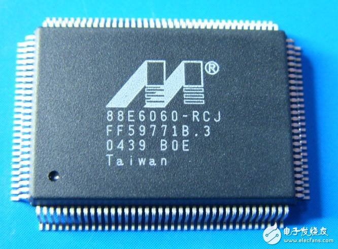
The Marvell®88 e6060 integrates a full 6-port Fast Ethernet switch on a single chip to support a single CPU connection. It contains five 10 base-t / 100 base-tx transceivers (physical), two can be used to support 100 base-fx; six independent Fast Ethernet media access control (mac), high-speed non-blocking switch architecture, high Performance address lookup engine and 1/2 m frame buffer mem-ory. It is a router designed for manufacturers with low port count switching systems and firewalls.
PHY transceiver design and advanced cable diagnostics with Marvell Vir-tual Cable TesterTM (VCTTM) technology. VCT allows IT managers to easily identify cabling problems to one meter and reduce network installation and support costs.
The Marvell 88E6060 is designed to work in all environments, supporting true plug and play in automatic crossover, automatic polarity and auto-negotiation of PHYs, and bridge loop prevention (using port state supported across tree). The shared memory-based switch fabric uses the latest Marvell switch architecture to provide non-blocking switching performance in all traffic environments.
The sixth port is the interface of the RMII / MII / MII / MII / SNI interface, which can be directly connected to the management or router cpu, which can be in RMII mode, MII-phy, MII-mac mode or MII-mac mode, or Is MII-mac mode, or MII-mac mode, these interfaces and BPDU operations, can be programmed for each port VLAN configuration, and port status, support spanning tree, truly isolated WAN and LAN firewall applications.
In Marvell 88E6060, Marvell's advanced mixed-signal processing technology enables digital implementation of adaptive equalization and clock data recovery, using special power management techniques to achieve low power consumption and high port count integration in Marvell 88E6060 The PHY and MAC units make full use of the relevant parts of the IEEE 802.3, IEEE 802.3 u and IEEE 802. 3x standards.
Many of the operating modes of the Marvell 88E6060 can be configured using SMI (Serial Management Interface - MDC/MDIO) and/or low cost serial EEPROM (93C46, C56 or C66).
88e6060 pin diagram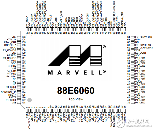
P[4:0]_RXP: Normal input, output in cross mode.
Accept the positive input,
P[4:0]_RXN: Normal input, output in cross mode.
Accept the input negative,
P[4:0]_TXP: Normal output, input in cross mode.
Accept the positive input,
P[4:0]_TXN: Normal output, input in cross mode.
Accept the input negative,
P[1::0]_SDET: input
Signal detection input. If port 0 and / or 1 are configured in 100BASE-FX mode, SDET indicates whether the signal of the fiber transceiver is detected, and the signal indicated by the positive level is detected.
If port 0 and/or 1 10/100BASE-T mode are configured, SDET is not used, but cannot be left floating because these pins do not contain internal resistors and must be connected to VSS or VDD directly through a 4.7K resistor.
P[1:0]_CONFIG: input
Configuration of ports 0 and 1. The CONFIG pin is used to set the default configuration for ports 0 and 1. These pins are connected to other device pins as follows:
VSS = Enable auto-negotiation - default
P0_LED1=force 10BASE-T half duplex
P0_LED2=Forced 10BASE-T full duplex
P1_LED0=force 100BASE-TX half duplex
P1_LED1=Forced 100BASE-TX full duplex
P1_LED2=force 100BASE-FX half duplex
VDDO=force 100BASE-FX full duplex
The default configuration for ports 2, 3, and 4 is auto-negotiation.
The CONFIG pin is configured after reset and contains internal pull-down resistors so they can be left floating to select auto-negotiation.
CONFIG_A: Internal pull-up resistor is set to mode 3 when the input is left floating
Global Configuration Pins: Global Configuration for Setting the Default LED Mode and Remote Fault Indication (FEFI) In 100BASE-FX mode, these pins are connected to other device pins as follows:
VSS= LED mode 0, FEFI disabled
P0_LED0= LED mode 0, FEFI
P0_LED1= LED mode 1, FEFI disabled
P0_LED2= LED mode 1, FEFI
P1_LED0= LED mode 2, FEFI disabled
P1_LED1= LED mode 2, FEFI
P1_LED2= LED mode 3, FEFI disabled
VDDO= LED mode 3, default FEFI enabled
The internal pull-up resistor is included after the CONFIG_A pin configuration is reset.
CONFIG_B: Input
Global configuration B, the global configuration pin is used to set the default automatic cross mode to; VDDO = automatic crossover, class B drive, energy detection enabled by default
Configured after reset, there is a pull-up resistor inside.
Voltage regulator and reference:
RSETP, RSETN: Reference resistor. A 2kΩ (1%) resistor is placed between RSETP and RSETN. This resistor is used to set an internal bias reference current.
CONTROL_15:
Voltage control of an external 1.5V regulator. This signal controls the external PNP transistor to generate a 1.5V supply for the VDD and VDDAL pins. CONTROL_25:
Voltage control of an external 2.5V regulator. This signal generates a 2.5V supply to control an external PNP transistor for the VDDAH pin.
system:
XTAL_IN: Input 25M crystal
25M or 50M system reference clock input; this clock input frequency is selected by CLK_SEL.
The clock source can come from the crystal's frequency (25 MHz) or the oscillator generator (25 or 50 MHz). This is only needed because it is used for the clock on the switch and PHY.
XTAL_OUT: Output 25M crystal
System reference clock output. This output can only be used to drive the frequency of an external crystal (25 MHz). It cannot be used to drive external logic. This pin should be left floating if the oscillator is connected to XTAL_IN.
CLK_SEL: Output to VSS
Clock frequency selection, this pin is connected to VSS if XTAL_IN is 25 MHz. If XTAL_IN is 50 MHz, this pin is tied to VDDO or left floating. This pin must be stable after reset.
CLK_SEL is pulled high by an internal resistor.
RESETn: Input reset low is valid
Hardware reset. Active low. 88E6060 configured at reset;
When RESETN is low, all pins are configured with inputs and the values ​​on these pins are latched on the rising edge of RESETN or after a period of time.
Register access interface:
MDC: The reference clock for managing data is the Serial Management Interface (SMI).
It is not expected to be a continuous clock stream, supporting a maximum frequency of 8.3 MHz.
SMI is used to access the physical layer (PHY) and registers in the switch if the serial EEPROM cannot access the registers. It can be SW_MODE[1:0] in all combinations.
The MDC is pulled high by an internal pull-up resistor.
MDIO: input;
Manage data input/output for SMI.
MDIO is used to transmit management data input and output synchronized with MDC;
This pin requires an external pull-up resistor in the range of 4.7kΩ to 10kΩ.
The 88E6060 device uses 16 possible SMI port addresses for 16.
This 16 can be used to select the EE_CLK/ADDR4 pin.
MDIO is pulled high by an internal pull-up resistor.
INTn: open drain output;
INTn is an active-low, open-drain output pin that indicates a non-maskable interrupt event.
When this signal is inactive, an external pull-up resistor is required to achieve a logic high.
Serial EEPROM interface:
EE_CS/EE_1K: I/O port, serial EEPROM chip selection
EE_CS is pulled high by an internal pull-up resistor. Use a 4.7kΩ resistor to VSS with low configuration
EE_CLK/ADDR4 : I/O, serial EEPROM clock
EE_CLK is pulled high by an internal pull-up resistor. Use a 4.7kΩ resistor to VSS configuration low.
EE_DIN/HD_FLOW_DIS: usually input,
EE_DIN is a versatile pin that is used to configure the 88E6060 during a hardware reset. When the chip is reset, the pin state is determined. When the chip is reset, EE_DIN becomes the input and the configuration disables the half-duplex flow control. Its value is latched on the rising edge of the reset.
Low = Enable flow control for all half-duplex ports
High=Disable flow control for all half-duplex ports
EE_DIN is pulled high by an internal resistor. Use a 4.7kΩ resistor to VSS configuration low.
HD_FLOW_DIS is used to select flow control for full-duplex ports
EE_DOUT: input
Serial EEPROM data from the EEPROM device.
EE_DOUT is the serial EEPROM data, reference EE_CLK is used to receive the EEPROM configuration data from the external serial EEPROM (if any).
EE_DOUT is pulled high by an internal resistor
Port 5 is enabled:
ENABLE_MII5: input;
Enable port 5MII mode, enable when high level, disable low level, internal pull-up resistor pulls high;
Port 5 works in MII mode:
P5_INCLK: general purpose I/O port: working in MAC mode
Input clock, this clock is reference P5_INDV and P5_IND[3:0], the direction and frequency of P5_INCLK are determined by P5_MODE[3:0] after the end of reset; if the port is in PHY mode, P5_INCLK is output. The clock frequency in 100BASE-X mode is 25 MHz, if the port is at 2.5 MHz in 10BASE-T mode and 50MHz RMII mode clock frequency.
If the port is in MAC mode, P5_INCLK is an input. The clock frequency in this mode can be anywhere from 0Hz to 25MHz, although it should be in 25MHz100BASE-X mode and 2.5MHz in 10BASE-T mode.
P5_INCLK is tri-stated during reset and it has an internal resistor pulled high.
P5_IND[3:0] input;
Input data. The data nibble received by P5_IND[3:0] is sent to the switch to select 100BASE-X and 10BASE-T modes;
P5_IND[3:0] is the synchronized P5_INCLK.
The inputs to these pins are derived from the mode of the port (ie mode PHY or MAC mode).
P5_IND0 SNI mode is used when it is selected.
P5_IND[1:0] Used when the RMII mode is selected.
The internal pull-up resistor of P5_IND[3:0] passes high.
P5_INDV: Input
The input data is valid.
When P5_INDV is set high, data P5_IND[3:0] is accepted by the switch. P5_INDV must be synchronous P5_INCLK SNI and MII mode, it must be synchronized to P5_OUTCLK or P5_INCLK in RMII mode.
P5_INDV pulls the resistor low internally.
P5_OUTCLK: General Purpose I/O
Input clock, this clock is reference P5_OUTDV and P5_IOUTD[3:0], the direction and frequency of P5_OUTCLK are determined by P5_MODE[3:0] after the end of reset;
If the port is in PHY mode, P5_OUTCLK is output. The clock frequency in 100BASE-X mode is 25 MHz if the port is 2.5 MHz in 10BASE-T mode and 50MHz RMII mode clock frequency.
If the port is in MAC mode, P5_OUTCLK is an input. The clock frequency in this mode can be anywhere from 0Hz to 25MHz, although it should be in 25MHz100BASE-X mode and 2.5MHz in 10BASE-T mode.
P5_OUTCLK is tri-stated during reset and it has an internal resistor pulled high.
P5_OUTD[3:0]/P5_MODE[3:0]: Usually the output is only input when resetting;
Output Data. And data transmitted by the switch;
The P5_OUTD[3:0] pins are synchronized to P5_OUT_CLK.
These pins are the mode of the output port (ie PHY or MAC mode).
Only P5_OUTD0 contains meaningful data in SNI mode
When P5_OUTD[1:0] selects RMII mode 1.
At reset, the value of the pin is locked to determine the operating mode and the internal resistor is pulled high;
P5_OUTDV: output
The output data is valid.
When P5_OUTDV is set high, data P5OUTD[3:0] is accepted by the switch.
P5_OUTDV must be synchronous P5_INCLK in MII mode, in RMII mode should be synchronized with P5_INCLK or P5_OUTCLK;
P5_INDV is tri-stated at reset and internally pulled high.
P5_CRS: General Purpose I/O
Carrier sense. After reset, if this port PHY mode is selected, P5_CRS becomes the output.
It is still the input if the MAC mode is selected.
P5_CRS will be set (or expected to be set to 1) when the receive data path is not idle.
P5_CRS is also set (or expected to be set) during transmission in half-duplex mode.
P5_CRS is asynchronous to P5_OUTCLK and P5_INCLK.
P5_CRS is tri-stated during reset, it is pulled low internally, so the pin can be left unconnected.
P5_COL: General Purpose I/O
collision. After reset, the PHY mode of P5_COL becomes the output, if this port is selected in the MAC mode selection. It is still an input;
In PHY mode, P5_COL is set to 1 when the transmit and receive paths are not idle in two half and full duplex modes; in half duplex MAC mode, P5_COL will be set to 1 non-idle transmit and receive paths.
In full-duplex MAC mode, P5_COL is ignored.
P5_COL is asynchronous with P5_OUTCLK and P5_INCLK.
P5_COL is tri-stated during reset and it is internally pulled low.
Port 4 enable: input;
DISABLE_MII4:
Disable port 4, enable PHY disable MII when high level, disable PHY enable MII when low level;
Internal pull-up resistor
Switch configuration port:
SW_MODE[1:0] output;
Switch mode. These pins are used to reset the 88E6060. The switch mode pin works as follows:
0 0 CPU connection mode, port is disabled
0 1 reserved
1 0 Stand-alone mode - ignore EEPROM
1 1 EEPROM connection mode 2
A CPU can be used in the EEPROM connection mode (SW_MODE[1:0] = [1, 1]). However, in all independent modes, the INTn pin asserts active low after the EEPROM initializes the internal registers (ie, the stop command has been executed);
The reset of the SW_MODE[1:0] rising edge is not latched and the correct device operation must remain static. They are pulled up by internal pull-up resistors.
FD_FLOW_DIS input
Full duplex flow control is disabled.
High=Disable flow control for all full-duplex ports
Low = Enable IEEE802.3x paused flow control on all supported full duplex ports
The rising edge of FD_FLOW_DIS to the PHY register reset of all ports is latched. It is pulled up by a resistor.
EE_DIN/ HD_FLOW_DIS multi-function pin selects half-duplex port flow control
Port status light:
P[4:0]_LED2 output
Each port is connected in parallel with the LED output, and the active-low LED pin directly drives the LED in parallel LED mode. It can be configured to display multiple options.
P [4:0]_LED2 is active low regardless of whether RESETN is set or not.
P[4:0]_LED1 output
Each port is connected in parallel with the LED output, and the active-low LED pin directly drives the LED in parallel LED mode. It can be configured to display multiple options.
P [4:0]_LED1 is active low regardless of whether RESETN is set or not.
P[4:0]_LED0 output
Each port is connected in parallel with the LED output, and the active-low LED pin directly drives the LED in parallel LED mode. It can be configured to display multiple options.
P [4:0]_LED0 is active low regardless of whether RESETN is set.
LEDSER:
The LEDSER output serial status bit is shifted into the shift register and can be displayed by the LED. LEDSER is the synchronous output LEDCLK.
LEDENA:
LEDENA is set to 1 regardless of whether the LEDSER is stored to the shift register has a valid state; LEDENA is synchronized to LEDCLK;
LEDCLK:
LEDCLK is the reference clock for the serial signal of the LED.
|
S/N
|
Project
|
General Parameter
|
|
1
|
Number of series
|
15S
|
|
2
|
Rated voltage
|
48V
|
|
3
|
End of discharge voltage
|
40V
|
|
4
|
Charging voltage
|
Recommend 51V (50.5V – 51.5V) for floating charge
Recommend 54V (53.5V – 54.5V) for equation charge |
|
5
|
Continuous charge and discharge curren
|
≤100A
|
|
6
|
Internal resistance (battery pack)
|
≤100mΩ
|
|
7
|
Self-discharge rate
|
≤2%/month
|
|
8
|
range of working temperature
(≤95%R.H.) |
0~65℃ charge
-20~65℃ discharge |
|
9
|
Storage temperature range(≤95%R.H.)
|
-40~70℃
|
|
10
|
Positive and negative lead way
|
Fence Terminal 2P*2
|
|
11
|
Display screen
|
LED display, four physical buttons
|
|
12
|
Protective function
|
Overcharge, over discharge, short circuit, overload, over temperature, etc.
|
|
13
|
certificate
|
MSDS,ISO9001,CE,UN38.3,ROSH
|
LIFEPO4 Battery For Home Energy Storage
Jiangsu Zhitai New Energy Technology Co.,Ltd , https://www.jszhitaienergy.com