
Analog-to-digital conversion is a critical process that transforms continuous analog signals into discrete digital values, offering an approximation of the original signal. This transformation involves quantization, where the analog signal is represented in binary form using bit-by-bit encoding. Currently, this process is executed through hardware implemented by ADC (Analog-to-Digital Converter) chips. The control mechanisms for these chips can be configured using different approaches such as DSP (Digital Signal Processor), ASIC (Application-Specific Integrated Circuit), or FPGA (Field-Programmable Gate Array), depending on the system's specific needs. Among these, the FPGA approach is particularly well-suited for high-speed and programmable environments. In this design, the Xilinx Spartan3E FPGA is used to manage and execute the analog-to-digital conversion function of the TI ADS1256 chip.
ADS1256 Chip IntroductionThe ADS1256 is a high-speed, low-noise 24-bit analog-to-digital converter that provides a complete solution for high-resolution analog signal measurement. It features a filter-stable buffer and a programmable gain amplifier, which help reduce noise and improve signal integrity. The chip supports a sampling rate of up to 30 kSps, making it suitable for applications requiring compliance with sanitary and phytosanitary standards. In terms of interface, the ADS1256 offers an SPI-compatible 5V serial interface. It accepts an analog input voltage of 5V and outputs digital signals ranging from 1.8V to 3.6V. The power consumption is relatively low, at 38 mW in standard mode and only 0.4 mW in standby mode.
Overall and Interface DesignThe input and output interface of the control system implemented by the FPGA is illustrated in Figure 3. One end connects to the ADS1256 chip, while the other end processes the digital output from the chip, combining it into 24-bit precision data for further use by the designer’s system.
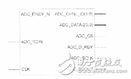
(1) CLK: Connects to the external 20MHz system clock to drive the FPGA;
(2) ADC_DRDY_N: A/D conversion ready signal connected to the /DRDY pin of the ADS1256, indicating when the conversion is complete;
(3) ADC_SDIN: SPI serial data output from the FPGA, used to configure the ADS1256 chip registers;
(4) ADC_CHNL_ID (1:0): Selects the input channel after A/D conversion, connected to D0 and D1 of the ADS1256.
Output:(1) ADC_CS: Chip enable signal connected to the /CS pin of the ADS1256;
(2) ADC_DATA (23:0): Parallel output for the final 24-bit data, which can be connected to other devices;
(3) ADC_D_RDY: Indicates when ADC_DATA is valid;
(4) ADC_SCLK: SPI clock derived from the main system clock, connected to the SCLK pin of the ADS1256;
(5) ADC_SDOUT: SPI serial data input from the ADS1256, connected to the FPGA’s input.
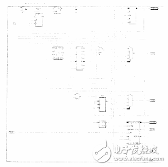
Function RealizationThe overall module design includes several sub-functions, such as the clock generation module “clk_gen,†which divides the 20MHz main clock to generate a 2MHz clock with a 50% duty cycle and a 4MHz clock for the SPI interface. The delay module “delay_n†introduces a time delay after system startup to ensure stable power supply before initialization. The “adc_initial†module initializes the ADS1256 via the SPI interface according to its specifications. The “adc_xchange†module controls the timing, sends control words, and reads the converted data based on the chip’s indications.
The RTL structure of the ADS1256 controller implemented on the FPGA is shown below:
This design utilizes the Xilinx primitive SRL16E to create a 16-bit shift register for clock control. The number of output bits can be calculated using the formula: Number of data output bits = 8*A3 + 4*A2 + 2*A1 + 1*A0 + 1. For example, with a 20MHz system clock, dividing it by 5 to achieve a 4MHz SPI clock requires setting A3, A2, A1, and A0 to 0, 1, 0, and 0 respectively (8*0 + 4*1 + 2*0 + 1*0 + 1 = 5).
By using SRL16E instead of a PLL for clock division, the design saves valuable FPGA resources. Each LUT in the FPGA can be configured as a 16-bit shift register, allowing the system to implement a 16-bit synchronous RAM. This technique is used to design a recursive delay line (RDL), which is then combined with time-division multiplexing to create a recursive folding structure. This approach increases the sampling rate and throughput without significantly increasing the main clock frequency, while drastically reducing resource usage.
In this design, a 1/4 recursive folding structure is employed, reducing resource consumption to just one-third of the previous design. As shown in the figure below, this optimization leads to efficient use of FPGA resources.
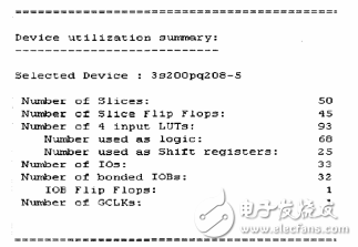
FPGA resource usage.
Alloy Products,Tantalum Alloy Wires,Aluminum Alloy Products,Alloy Custom Products
Shaanxi Xinlong Metal Electro-mechanical Co., Ltd. , https://www.cnxlalloys.com