
The clock device design utilizes an I2C-programmable fractional phase-locked loop (PLL) to meet high-performance timing requirements, ensuring a frequency with zero PPM (parts per million) of synthesis error. High-performance clock ICs feature multiple clock outputs that drive various subsystems in applications such as printers, scanners, and routers—like processors, FPGAs, and data converters. These complex systems often require dynamic updates to the reference clock frequency to support protocols like PCIe and Ethernet.
The clock IC functions as an I2C slave, requiring the host controller to configure its internal PLL logic. This control logic can be written to the microcontroller, which acts as an I2C master. The microcontroller configures the volatile memory within the clock IC and controls the PLL, enabling dynamic updates to the system clock frequency through the onboard MCU-IC combination. Programmable microcontrollers provide the necessary control logic for high-performance clock ICs, resulting in a more compact system design and reduced material costs by minimizing the number of on-board ICs and traces.
Theory of Operation
Figure 1 illustrates the basic PLL architecture used in high-performance clock devices. This design uses a scaling factor to generate the desired output frequency from the PLL. The final output frequency is calculated using the following formula:
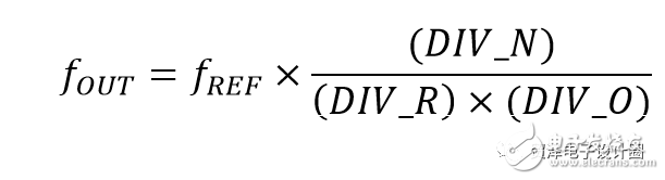
Here, fREF represents the input reference crystal frequency, typically ranging from 8 MHz to 48 MHz. DIV_R (including DIV_R1 and DIV_R2) refers to the prescaler division factor, while DIV_N is the fractional-N factor. Finally, DIV_O (such as DIV-O1, DIV-O2, etc.) is the post-divider factor before the output signal is generated.
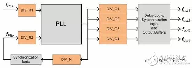
Figure 1: Simplified PLL block diagram for a high-performance clock
The orange block in Figure 1 represents programmable parameters, and the equations involving these parameters are also programmable. These settings are stored in the non-volatile memory of the clock device at the factory. The device includes both volatile and non-volatile memory, with the latter being copied into the former during power-up. This ensures that the PLL generates the correct default clock output upon initialization.
One key feature of the clock IC is runtime programming via the I2C interface. This allows users to modify the volatile memory contents instantly, enabling real-time changes to the system configuration. The host controller can send appropriate I2C commands to implement these changes quickly.
Additionally, the non-volatile memory can store multiple user configurations. Users can select one of these pre-defined profiles using the Frequency Select (FS) pin. This CMOS input pin receives an external N-bit signal, which then selects a specific configuration from the non-volatile memory. Once selected, this configuration is copied to the volatile memory, and the PLL adjusts accordingly to produce a different output signal.
Meanwhile, the microcontroller provides data over I2C to control the high-frequency clock. Its advantage lies in its variety of communication peripherals, including I2C, SPI, UART, Bluetooth, and ZigBee, allowing it to interact with other microcontrollers or transfer data to Android and iOS devices. The availability of development tools further simplifies the design process, making it ideal for implementing custom applications through I2C instructions.
High-performance Clock Application Requirements
High-performance clock ICs are designed for use in consumer, industrial, and networking applications. They offer multiple differential and single-ended outputs derived from different PLLs and are programmable via the I2C interface. These ICs also support critical interface standards like PCI Express (PCIe), USB, and 10 Gigabit Ethernet. Additional features such as voltage-controlled crystal oscillators (VCXO) and frequency selection (FS) are also supported.
The high-performance clock IC operates in I2C slave mode, requiring an onboard I2C host to manage the following programmable features:
- In-system programming via I2C interface
- Configuration updates via the FS pin
- External reset operation
- Voltage-controlled crystal oscillator (VCXO) operation

Figure 2: Microcontroller - High Performance Clock Interface Circuit
The Role of Microcontrollers in Clock IC PLL Control
As shown in Figure 2, the clock IC is connected to the microcontroller circuit. The internal PLL block generates a tuning voltage (Vtune) based on the frequency band. The PLL module receives the local oscillator frequency, amplifies it, and passes it to the phase comparator after downconversion via the prescaler.
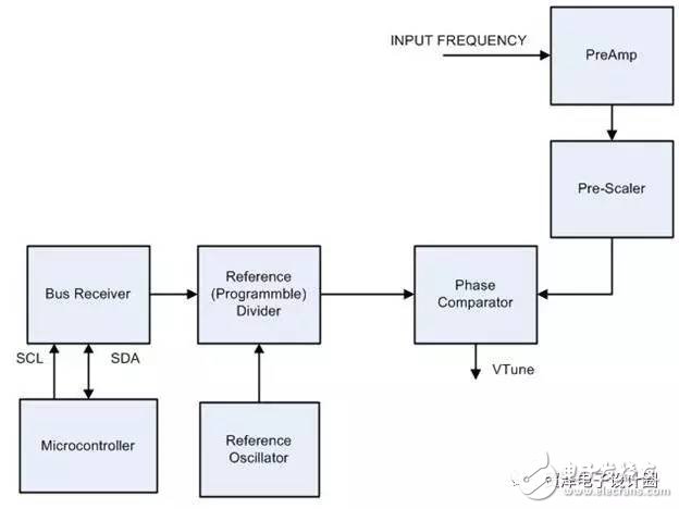
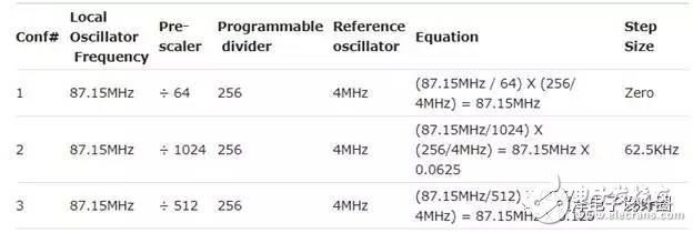
Figure 3: Microcontroller Control for the PLL Module
The microcontroller sends data to the programmable divider through I2C. The divider also receives input from a reference oscillator, such as a 4 MHz crystal. The phase comparator compares the local oscillator frequency (e.g., 87.15 MHz) with the reference frequency (also 87.15 MHz). If they match, the phase comparator produces the Vtune voltage. A mismatch leads to no valid output. Figure 3 shows the full block diagram.
With the help of the microcontroller, the PLL forms a closed-loop system, generating a tuning voltage that increases as the frequency increases. The microcontroller can adjust the step size by modifying the prescaler and programmable divider values.
Step size = (local oscillator frequency / prescaler) × (programmable frequency divider / reference oscillator)
Table 1 shows some example configurations.
In-system Programming via the I2C Interface
In-system programming enables rapid and efficient system design iterations. Programming data is transferred via the SCL and SDA pins, and the sequence of operations is programmed into the onboard microcontroller (master), which interacts with the slave clock device at runtime using commands and data.
For example, consider a system where the clock signal must be a multiple of the sample rate. The required frequency may vary between 155.52 MHz and 156.25 MHz. The microcontroller can access and update the PLL configuration in volatile memory to meet these two frequency requirements dynamically.
Update Configuration via Frequency Selection (FS) Pin
High-performance clock devices support multiple user profiles with customizable configurations. The FS pin allows for two types of switching: fast and slow. Fast switching is used for output ON/OFF, crossover value changes, and MUX setting adjustments, while slow switching is suitable for changing PLL parameters, including ON/OFF states. As the names suggest, fast switching results in quicker output changes, while slow switching is slower but still reliable. Both modes allow for safe on/off transitions without errors. Figure 4 illustrates the timing relationship between the FS pin and the output clock.
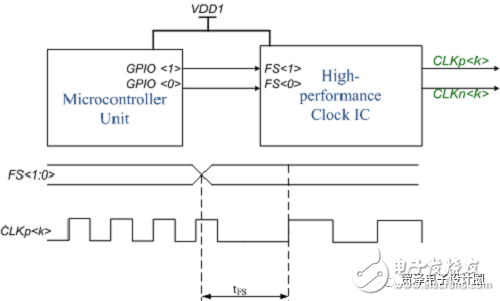
Figure 4: Frequency Selection Operation
External Reset Operation
When an external reset is applied, the clock IC enters low-power mode. The output and I2C bus signals go into a high-impedance (HI-Z) state until the reset is released and initialization completes. The external reset clears the volatile memory, and the non-volatile memory configuration is copied back. This feature is useful when reinitializing an application running on any system.
Voltage Controlled Crystal Oscillator (VCXO) Operation
In some applications, the output clock frequency must track the input data stream using analog feedback. As shown in Figure 5, the clock IC is part of a larger phase-locked loop. The ASIC or SoC tracks the input stream, calculates the error, generates a PWM signal, and feeds it back to the local clock generator for frequency tuning.
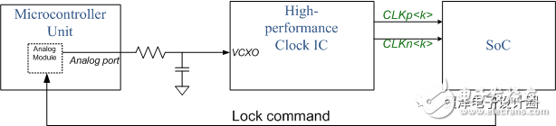
Figure 5: VCXO Example Circuit
The VCXO function allows the PLL frequency to be adjusted independently of crystal characteristics, temperature, voltage, or manufacturing process. VCXO modulation is linear and precise. A clock reference can also be used. With the built-in analog module of the microcontroller, the VCXO control logic can be accurate up to six decimal places.
As an I2C master, the microcontroller configures the volatile memory of the clock IC and controls the PLL. This allows dynamic updates to the system clock frequency through the onboard MCU-IC combination. Developers can use programmable microcontrollers to provide control logic for high-performance clock ICs, reducing the need for additional on-board components and making the overall design more compact.
The microcontroller comes with powerful IDE tools that accelerate application development. Integrated Programmable System-on-Chip (PSoC) devices further simplify the design and help reduce overall product cost. For more details on high-performance clock IC design, click here to read and download "4-PLL Spread Spectrum Clock Generator Getting Started."
Connector 2.5Mm Pitch,S11 Connectors,Welding Bar Connectors,Pressure Weld Bar Connector
YUEQING WEIMAI ELECTRONICS CO.,LTD , https://www.wmconnector.com