
Industrial Router Crystal 3.2*2.5mm 3225 26M (26.000MHZ) 12PF 10PPM 20PPM 30PPM
Inductance and Capacitance Components
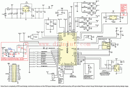
 The following is the circuit diagram of [ADNS7630 application circuit diagram].
The ADNS-7630 is a high-performance laser navigation sensor integrated with a Bluetooth 2.1 system-on-chip (SoC). It is compatible with the Bluetooth HID form factor V1.0 and Bluetooth Low Energy (BLE) V2.1, making it ideal for wireless input devices. The chip is also safe to use under IEC/EN 60825-1 Class 1 eye safety standards. With a motion detection speed of up to 30 inches per second and an acceleration capability of up to 8g, this device offers excellent responsiveness and precision.
It supports up to 10 I/O pins, allowing for flexible integration into various applications. The 4-axis sensor rotation feature enables orientation adjustments at 0°, 90°, 180°, or 270°, enhancing usability in different scenarios. The resolution can be programmed from 250 to 3000 CPI (counts per inch), with increments of 250 CPI per step, providing users with customizable sensitivity settings.
This component is widely used in Bluetooth-enabled wireless laser mice and other integrated input devices, offering a balance between performance, power efficiency, and reliability. Whether for gaming, office use, or general computing, the ADNS-7630 delivers accurate tracking and smooth operation.
The following is the circuit diagram of [ADNS7630 application circuit diagram].
The ADNS-7630 is a high-performance laser navigation sensor integrated with a Bluetooth 2.1 system-on-chip (SoC). It is compatible with the Bluetooth HID form factor V1.0 and Bluetooth Low Energy (BLE) V2.1, making it ideal for wireless input devices. The chip is also safe to use under IEC/EN 60825-1 Class 1 eye safety standards. With a motion detection speed of up to 30 inches per second and an acceleration capability of up to 8g, this device offers excellent responsiveness and precision.
It supports up to 10 I/O pins, allowing for flexible integration into various applications. The 4-axis sensor rotation feature enables orientation adjustments at 0°, 90°, 180°, or 270°, enhancing usability in different scenarios. The resolution can be programmed from 250 to 3000 CPI (counts per inch), with increments of 250 CPI per step, providing users with customizable sensitivity settings.
This component is widely used in Bluetooth-enabled wireless laser mice and other integrated input devices, offering a balance between performance, power efficiency, and reliability. Whether for gaming, office use, or general computing, the ADNS-7630 delivers accurate tracking and smooth operation.
Cutting Machines,Cloth Cutting Machine,Laser Cutter,Cutter Machine Machine
Kunshan Bolun Automation Equipment Co., Ltd , https://www.bolunmachinery.com