
Summary:
Abstract: This application note provides guidance and recommendations for radio frequency (RF) printed circuit board (PCB) design and layout, including some discussion of mixed-signal applications. The material provides a “best practice†guide that should be applied in conjunction with all other design and manufacturing guidelines that may apply to specific components, PCB manufacturers, and materials.
table of Contents
Introduction RF transmission line
-microstrip line
- Stripline
- Coplanar waveguide (ground)
- Characteristic impedance
- Transmission line angle compensation
-Transmission line change layer Signal line isolation Grounding area Special considerations for bias and ground plane Power (bias) trace and power supply decoupling Decoupling and bypass capacitor selection Bypass capacitor layout considerations Short circuiter connection component ground
IC grounding area ("pad")
This application note provides guidance and recommendations for radio frequency (RF) printed circuit board (PCB) design and layout, including some discussion of mixed-signal applications, such as digital, analog, and RF components on the same PCB. Content is organized by topic and provides a “best practice†guide that should be applied in conjunction with all other design and manufacturing guidelines that may apply to specific components, PCB manufacturers, and materials.
RF transmission line
Many Maxim RF components require an impedance controlled transmission line that transmits RF power to (or transmits power from) IC pins on the PCB. These transmission lines can be implemented in the outer layer (top or bottom layer) or buried in the inner layer. Guidance on these transmission lines includes discussion of microstrip lines, strip lines, coplanar waveguides (ground), and characteristic impedance. It also introduces the transmission line corner compensation and the layer change of the transmission line.
Microstrip lines This type of transmission line includes fixed-width metal traces (conductors) and ground planes directly below (adjacent layers). For example, traces on the first layer (top metal) require a solid grounded area on the second layer (Figure 1). The width of the trace, the thickness of the dielectric layer, and the type of dielectric determine the characteristic impedance (typically 50Ω or 75Ω).
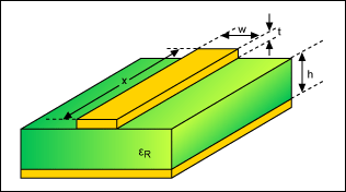
Figure 1. Example of a microstrip line (stereo)
Stripline This line consists of a fixed width of the inner layer and a grounding area above and below. The conductor can be located in the middle of the grounded area (Figure 2) or with a certain offset (Figure 3). This method is suitable for the inner layer of RF traces.
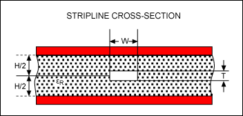
Figure 2. Stripline (end view).
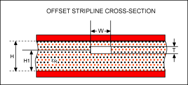
Figure 3. Offset stripline. A variant of the stripline for PCBs with different layer thicknesses (end view).
Coplanar waveguide (ground)
Coplanar waveguides provide better isolation (end view) between adjacent RF lines and other signal lines. This medium consists of an intermediate conductor and grounded areas on both sides and below (Figure 4).
Figure 4. Coplanar waveguides provide better isolation between adjacent RF lines and other signal lines.
It is recommended to install a via "fence" on both sides of the coplanar waveguide, as shown in Figure 5. This top view provides an example of installing a row of ground vias on the top metal ground area on each side of the intermediate conductor. The loop current caused on the top layer is shorted to the ground plane below.
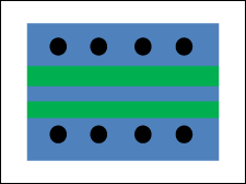
Figure 5. It is recommended to install a via fence on both sides of the coplanar waveguide.
Characteristic impedance  A variety of calculation tools are available to properly set the signal conductor linewidth to achieve the target impedance. However, care should be taken when entering the dielectric constant of the board layer. A typical PCB outer substrate layer contains a glass fiber component that is smaller than the inner layer, so the dielectric constant is low. For example, the dielectric constant of FR4 material is generally εR = 4.2, while the outer substrate (pre-cured) layer is generally εR = 3.8. The example below is for reference only, where the metal thickness is 1 oz copper (1.4 mils, 0.036 mm).
Table 1. Example of characteristic impedance

Transmission Line Bend Compensation When the transmission line is required to bend (change direction) due to wiring constraints, the bending radius used should be at least 3 times the width of the intermediate conductor. That is:
Bending radius ≥ 3 × (line width)This minimizes the characteristic impedance variation of the corners.
If it is not possible to achieve a gradual bend, the transmission line can be bent at a right angle (not curved), see Figure 6. However, this must be compensated to reduce the impedance jump caused by the increase in the local effective line width as it passes through the bend point. The standard compensation method is angle mitre, as shown in the figure below. The best microstrip right angle slanting is given by the Douville and James formula:
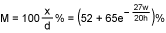
In the formula, M is the ratio (%) of the miter and non-mitted corners. This formula is independent of the dielectric constant and is constrained by w/h ≥ 0.25.
A similar method can be used for other transmission lines. If there is any uncertainty about the correct compensation method and the design requires a high performance transmission line, the electromagnetic simulator should be used to model the corners.
Figure 6. If it is not possible to achieve a gradual bend, bend the transmission line at right angles.
Layer Change of Transmission Lines If layout constraints require that the transmission line be changed to a different board layer, it is recommended to use at least two vias per transmission line to minimize the via inductance load. A pair of vias effectively reduces the transmission inductance by 50% and should use the largest diameter via that is equivalent to the transmission line width. For example, for a 15-mil microstrip line, the via diameter (polished plating diameter) should be 15 mils to 18 mils. If space is not allowed to use large vias, use three smaller transition vias.
Signal line isolation
Care must be taken to prevent accidental coupling between signal lines. The following are examples of potential coupling and preventive measures:
RF transmission line: The distance between transmission lines should be as large as possible and should not be close to each other over long distances. The smaller the spacing from each other, the longer the parallel trace distance, and the greater the coupling between the parallel microstrip lines. Traces on different layers should have grounded areas to keep them separate. Transmission lines carrying high power should be as far away as possible from other transmission lines. Grounded coplanar waveguides provide excellent line-to-line isolation. It is not practical to isolate the RF lines on a small PCB above about -45 dB.
High-speed digital signal lines: These signal lines should be placed independently on a different board layer than the RF signal lines to prevent coupling. Digital noise (from the clock, PLL, etc.) is coupled to the RF signal line and modulated onto the RF carrier. Or, in some cases, digital noise is upconverted/downconverted.
VCC/Power Cord: These wires should be placed on a dedicated layer. Appropriate decoupling/bypass capacitors should be installed at the primary VCC distribution node and the VCC branch. The bypass capacitor must be selected based on the overall frequency response of the RF IC and the expected frequency distribution of the digital noise caused by the clock and PLL. These traces should also be isolated from the RF line, which will emit large RF power.
Grounding area
If Layer 1 is used for RF components and transmission lines, it is recommended to use a solid (continuous) ground plane at Layer 2. For strip lines and offset strip lines, the grounding area is required for the upper and lower intermediate conductors. These areas must not be shared or assigned to a signal or power network, but must be allocated to the ground. Sometimes limited by design conditions, a local grounding area on a layer must be located below all RF components and transmission lines. The grounding area must not be disconnected below the transmission line.
A large number of ground vias should be placed between the different layers of the RF portion of the PCB. This helps prevent the ground current loop from causing an increase in parasitic ground inductance. Vias also help prevent cross-coupling of RF signal lines on the PCB from other signal lines.
Special considerations for power and ground planes
For board layers assigned to system power (DC power) and ground, the loop current of the component must be considered. The general principle is to avoid placing the signal lines on the board layer between the power plane and the ground plane.
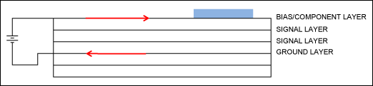
Figure 7. Incorrect board layer assignment: There is a signal layer between the power plane and the ground current loop on the ground plane. Bias line noise is coupled to the signal layer.
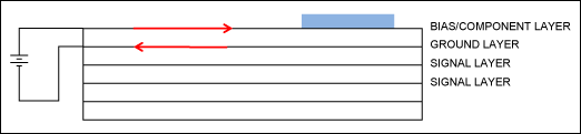
Figure 8. Better board layer assignment: There is no signal layer between the power plane and the ground plane.
Power (bias) trace and power supply decoupling
If the component has multiple power connections, it is common to use a "star" configuration of the power wiring (Figure 9). Install larger decoupling capacitors (tens of μF) at the “root†node of the star configuration and install smaller capacitors on each branch. The value of these small capacitors depends on the operating frequency of the RF IC and its specific function (ie, decoupling between the stages and the mains). The figure below shows an example.
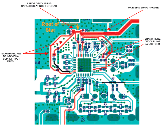
Figure 9. If the component has multiple power connections, the power wiring can be configured in a star configuration.
The "star" configuration avoids long ground loops relative to the configuration in which all pins connected to the same power network are connected in series. Long ground loops can cause parasitic inductance and can cause unexpected feedback loops. A key consideration in power supply decoupling is that the DC power connection must be electrically defined as an AC ground.
Decoupling and bypass capacitor selection
Due to the existence of a self-resonant frequency (SRF), the effective frequency range of the capacitor in reality is limited. SRFs are available from the manufacturer, but sometimes feature analysis must be performed by direct measurements. Above SRF, the capacitor is inductive and therefore does not have a decoupling or bypass function. If wideband decoupling is required, the standard practice is to use multiple capacitors with increased capacitance values, all in parallel. Small capacitors have a large SRF (for example, 0.2pF, 0402 SMT package capacitor SRF = 14GHz), and large capacitors have a small SRF (for example, SRF = 4GHz for the same package 2pF capacitor). Table 2 lists the typical configurations.
Table 2. Effective frequency range of the capacitor

Since the power line must be AC ​​ground, it is important to minimize the parasitic inductance of the AC ground loop. Component placement or placement may cause parasitic inductance, such as the ground direction of the decoupling capacitor. There are two ways to place the bypass capacitor, as shown in Figure 10 and Figure 11, respectively:
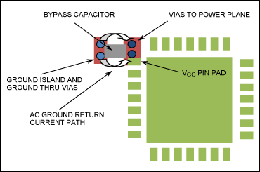
Figure 10. In this configuration, the total footprint of the bypass capacitor and associated vias is minimal.
In this configuration, connecting the VCC pads on the top layer to the vias of the inner power supply region (layer) may interfere with the AC ground current loop, forcing a longer loop, resulting in higher parasitic inductance. Any AC current flowing into the VCC pin goes through the bypass capacitor to its ground side and back to the internal ground plane. In this configuration, the total footprint of the bypass capacitor and associated vias is minimal.
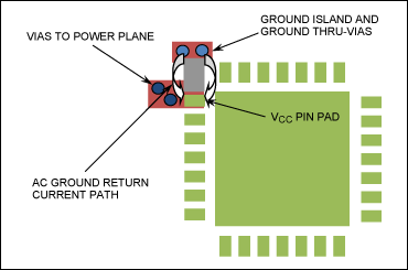
Figure 11. This configuration requires a large PCB area.
In another configuration, the AC ground loop is not limited by the vias in the power supply area. In general, this configuration requires a slightly larger PCB area.
Grounding of the shorting device connecting element
For components with shorted connections (grounded) (such as power supply decoupling capacitors), it is recommended to use at least two ground vias per component (Figure 12), which reduces the effects of via parasitic inductance. The short-circuit connection component group can use the via ground "island".

Figure 12. Using at least two ground vias per component reduces the effects of via parasitic inductance.
IC grounding area ("pad")
Most ICs require a solid ground area on the component layer (top or bottom of the PCB) directly below the component. The ground plane will carry DC and RF reflow and flow through the PCB to the assigned ground plane. The second function of the component "ground pad" is to provide a heat sink, so the pad should include the maximum number of vias as allowed by the PCB design rules. In the example shown below, a 5 × 5 via array is mounted on the intermediate ground area (on the component layer) directly below the RF IC (Figure 13). The maximum number of vias should be used where other layout considerations allow. These vias are ideal vias (through the entire PCB). These vias must be plated. If possible, fill the vias with thermal paste to improve thermal performance (fill the thermal paste after plating the vias and before plating the board).
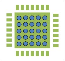
Figure 13. Place a 5 × 5 via array on the intermediate ground area directly below the RF IC
Customized PVC Bluetooth Charger
Shenzhen Konchang Electronic Technology Co.,Ltd , https://www.konchangs.com